
We use cookies to ensure our website works properly and to personalise your experience. Cookies policy
Electronics and Communication Engineering, National Institute of Technology Hamirpur, 177005, Himachal Pradesh, India
In this study, a high-throughput and low-latency Optimized DA-FIR filter architecture is proposed by integrating a optimized Approximate Karatsuba Multiplier (opt-AKM) and optimized Variable Latency-Reduced Carry Skip Adder (opt-VLCSA). The opt-AKM accelerates partial product computation using a combination of Booth Encoding, Wallace Tree reduction, and Carry-Save Adders, significantly reducing computational complexity. Meanwhile, the opt-VlCSA minimizes critical path delay through a carry propagation scheme combining carry-skip and carry-lookahead logic. To further enhance throughput, both opt-AKM and opt-VLCSA are implemented using a pipelined structure, resulting in improved parallelism and efficient resource utilization. Simulation and synthesis results confirm significant improvements in speed, power efficiency, and hardware resource utilization compared to conventional DA-FIR designs. The im-plementation is carried out using Verilog in Vivado 2024.1, and experimental evaluations demonstrate that the proposed Optimized DA-FIR filter integrated with opt-AKM and opt-VLCSA achieves reduced delay, lower static power consumption, and enhanced overall performance.
Digital Signal Processing (DSP). The usage of DSP for developing Digital FIR filters and there FPGA implementation. such as low-pass, high-pass, band-pass, band-stop filters along with Noise removal application in SDR. has developed as Distributed arithmetic-FIR filter design using Approximate Karatsuba Multiplier and VLCSA [1]. For developing electrical devices such as accelerators, sensors,and filters has developed as more effective [2]. In the application of recursive, the transverse filter, Fast Fourier Transform (FFT), Discrete Fourier Transform (DFT) and multiplier are operated in their integration [3]. The effectiveness of the (DSP) technique through suggestions for the arithmetical units of architectural design is valuable on its own [4]. According to recent research, an arithmetic method that includes data sharing procedures gives significant increases in speed based on mathematical optimization [5]. Moreover, the multiplier–low Finite Impulse Response (FIR)filter design replaces the development operations through various moved supplements, depending on the findings [6]. The linear and stable transition response is safeguarded through FIR filter that reduced the shared applicant in numerous Digital Signal Processing (DSP) applications [7]. Filters are applied in input signals frequency range, passive filters reduce the signal [8]. A filter is a tool that periodically reshapes the signal waveform [9]. The primary objective of digital signal processing filter is reduce noise, which improves signal efficacy and to eliminate adequate information as signal [10]. Various methods of filters are used to diminish the impact of noise [11]. The multiplication of Finite Impulse Response filters raises the clock frequency while decreasing area and power. A finite Impulse Response method needs a greatly sophisticated set of equality restrictions [12]. This complexity is diminished through multiplier-less FIR filters permit simplifying shift networks and add-ons to perform multiplication functions using various initiatives [13]. The aim of filter adaptation is to reduce the mean square error among the desired and filter output. DA architectures are employed to decrease the filter design complexity [14]. Two memory units are employed in the filter through multipliers to construct the DA structures, one to hold the filter product and another one to stock the updated weights [15]. Because the inclusion of multi pliers as well as adders increases the critical route time at the filter designing, the truncation based partial product generation is utilised [16]. The adaption latency is then minimized using a new partial product generator as well as an upgraded and stabilized pipeline structure [17]. The problems in the previous approaches are in applications, noise from the surrounding environment diminishes the quality of the voice and audio signal. Noise cancellation (NC) gained lots of attention as a system to eliminate speech signal containing noise to enhance the quality of speech and audio signal. The adaptive filter is a significant noise cancellation building block that delivers noise reduction in the absence of prior knowledge of noise and signal. Generally, there is a tradeoff among hardware complexity and filter performance linked with the word length of multipliers (usually coefficients). Increasing the co efficient word length increases the execution complexity, and decreases the coefficient word length outcomes at larger filter response error [18] [19] [9] [20] [21] [22]. This compensation is essential for the execution of entire filters. Therefore, effectual design is needed to attain noise reduction; reducing energy per operation (EPO), lower yields per area (TPA) is motivated to do this task
In this manuscript, High Throughput and Low Latency optimized DA-FIR filter design integrated with optimized Approximate Karatsuba Multiplier (opt-AKM) and optimized Variable Latency Carry Skip Adder (opt-VLCSA) is proposed for designing low pass filter application and its FPGA implementation . The primary contributions of this manuscript are summarizes as follows;
Designed and implemented a DA-FIR filter that integrates novel optimized modules (HE-AKM and HLR-CSA) for efficient signal processing.
Combined Booth Encoding, Truncated Multiplication, Wallace Tree, and Approximate Adders to reduce complexity, power, and delay in multiplication stages.
Implemented a hybrid carry-skip and carry-lookahead adder to minimize carry propagation delay and improve overall speed in accumulation stages.
Achieved significant reductions in delay (timing), power consumption, and area usage, compared to traditional DA-FIR implementations.
Verified filter performance using real-world sinusoidal and noisy audio signals, showing clear removal of unwanted frequency components.
Developed a methodology to extract filter coefficients from MATLAB and seamlessly integrate them into Verilog simulations, bridging software and hardware design.
Validated output waveform integrity and frequency isolation to ensure that signal distortion is minimized and filtering goals are met.
Modular Verilog code enables reuse of HE-AKM and HLR-CSA components in other DSP and VLSI systems beyond FIR filters.
The proposed filter architecture contributes to the field of efficient VLSI signal processing, especially in appli-cations requiring low latency and energy efficiency.
Motivation for Optimization Traditional FIR filters, while accurate and stable, often require a large number of multipliers and adders, leading to increased power consumption, area overhead, and processing delay—especially in high-tap or real-time filtering applications. Distributed Arithmetic (DA) addresses the need to eliminate conventional multipliers, but the performance bottleneck then shifts to the accumulation of partial products and their associated arithmetic operations.
Moreover, as FIR filters scale in size and precision (e.g., for audio, biomedical, or communication systems), the delay introduced by conventional multipliers and ripple-carry or fixed-latency adders becomes a significant concern. In such systems, achieving both speed and energy efficiency becomes critical, which cannot be achieved with standard arithmetic units alone.
This creates a strong motivation to optimize the arith-metic blocks within the DA-FIR architecture—specifically, the multiplier and the adder, using advanced and application-aware techniques. Key Contributions To address the above challenges, the following major contributions are made in this work:
A novel multiplier architecture is developed using a Karatsuba-based divide-and-conquer algorithm, which recur-sively splits input operands for more efficient multiplication. The multiplier integrates Booth Encoding, Wallace Tree Re-duction, Carry Save Adders (CSA), and Approximate Adders to reduce hardware complexity and power usage. The use of approximate adders exploits the error-tolerance nature of FIR filters in non-critical paths to trade off a small precision loss for significant performance gains.
A high-speed adder that combines the benefits of carry skip and carry select mechanisms. The VLCSA dynamically adjusts the carry propagation delay based on actual input conditions, thereby reducing average delay compared to fixed-latency adders. It is seamlessly integrated into the accumulator stage of the DA-FIR filter, improving both speed and power efficiency.
A complete FIR filter is designed using the optimized AKM and VLCSA components.
The architecture is described in Verilog HDL and synthe-sized in Xilinx Vivado.
Simulation results confirm correct filtering behavior with significant reductions in delay (up to 25 ns), power, and logic utilization compared to standard DA-FIR architectures.
This work therefore provides a high-speed, low-area, and energy-efficient FIR filter solution that is well-suited for real-time applications.
In high-speed and area-constrained VLSI systems, multi-plication is often the most resource-intensive operation. Tra-ditional multipliers such as array or shift-and-add methods suffer from high delay and power consumption, especially for wide operands. The Karatsuba algorithm offers a divide-and-conquer approach that reduces the number of partial products by recursively breaking large multiplications into smaller ones. However, even Karatsuba’s efficiency can be improved fur-ther for digital signal processing (DSP) applications—like FIR filters—where error tolerance allows for approximate comput-ing. By introducing approximate adders into non-critical paths and optimizing partial product generation and accumulation using Booth encoding and Wallace tree structures, significant gains in speed, area, and power are achieved.
The Optimized AKM
Karatsuba multiplication for recursive partitioning, Booth en-coding for reducing the number of partial products, Wallace tree and Carry-Save Adders (CSA) for fast accumulation, and Approximate Adders for resource-efficient summation. Input A and B (n-bits)are divided into two or more smaller segments using the kartasuba method.
A = A1 × 2n/2 + A0
B = B1 × 2n/2 + B0
Kartasuba Equations :
|
n |
where
P 0 = A0 × B0
P 1 = (A1 + A0) × (B1 + B0)
P 2 = A1 × B1
n is the width of input (8-bit or 16-bit input)
Internal Components:
The Booth Encoder reduces the number of partial products by encoding bits in groups, which is particularly effective for signed number multiplication. In Radix-4 Booth encoding, two bits are grouped to decide whether to multiply the multiplicand by 0, ±1, or ±2. This leads to fewer partial products, lowering the overall critical path and power usage. Reduce product using grouping
Group bit:
bi + 1, bi, bi − 1
Encoded Result :
0 if 000 or 111
+1 if 001 or 010
-1 if 101 or 110
+2 if 011
-2 if 100
The Wallace Tree is a parallel structure that reduces multiple partial products into two rows using full and half adders in a tree-like structure. It minimizes the height of the addition tree, thereby reducing delay.
CSAs are used to sum three or more operands simultaneously without immediately propagating carries. This speeds up multi-operand addition in the Wallace tree stage and prepares the data for final summation.
Approximate Adders provide faster and less power-hungry addition at the cost of minor inaccuracies, which are acceptable in DSP tasks. In AKM, they are used in final summation stages where bit-level precision is less critical.
Inputs A and B (n-bit) are divided into two or more smaller segments.
Each sub-multiplication utilizes Booth Encoding to mini-mize partial products, and a Wallace Tree to sum them quickly.
Partial products are accumulated using CSAs and finalized using approximate adders for faster output with minimal area and delay.
Final Output Composition: The final product is recon-structed as
P = P 2 × 2n + P 1 × 2n/2 + P 0
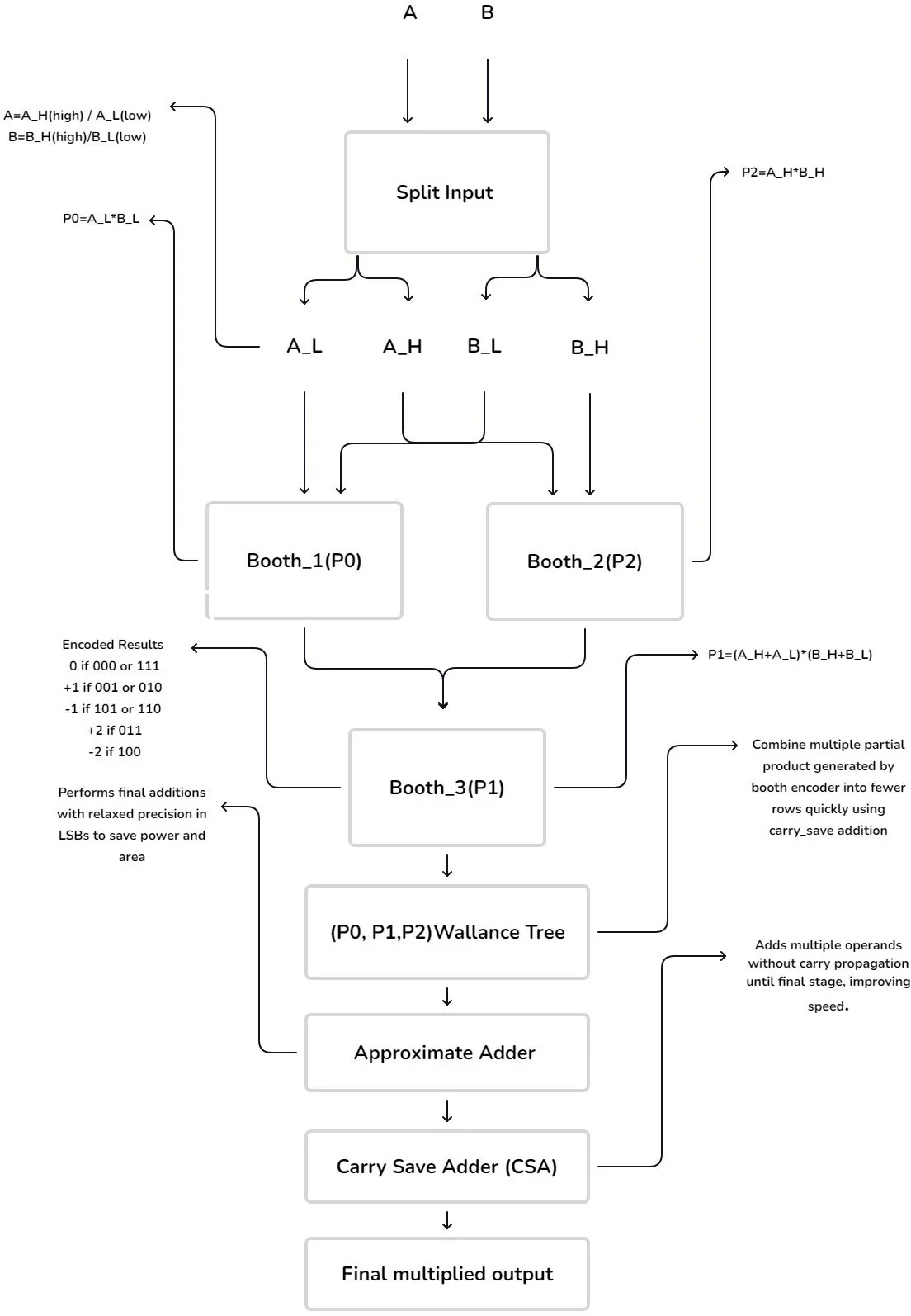
Fig. 1. Optimized Approximate Karatsuba Multiplier (AKM)
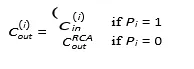
The VLCSA is used to speed up the addition process in the DA-FIR architecture. It combines the speed of Carry Skip Adder (CSA) with flexibility of Variable Latency control to reduce critical path delay.
Traditional Carry Skip Adders (CSA) improve speed over Ripple Carry Adders (RCA) by allowing fast propagation of carry bits through blocks of bits. However, they still suffer from uniform delay across blocks regardless of whether a carry skip is actually needed. This results in inefficient resource usage in variable switching conditions. VLCSA (Variable Latency Carry Skip Adder) addresses this inefficiency by enabling adaptive carry propagation based on input conditions. It introduces block-based segmentation, carry-skip logic, and a variable path latency model, significantly improving delay without increasing area or power consumption.
Optimized VLCSA Architecture and Working :
The VLCSA design Segmentation into Variable Blocks, The full input (e.g., 32 bits) is divided into smaller segments (e.g., 4 blocks of 8 bits each).
A[N − 1 : 0], B[N − 1 : 0]
There are N-bit operands (e.g., 16 bits) Block Splitter:
A = [A15 : 12, A11 : 8, A7 : 4, A3 : 0]
B = [B15 : 12, B11 : 8, B7 : 4, B3 : 0]
For a 16-bit adder,divide 4 block of 4-bits each
Generate (G), Propagate (P) logic to assess whether carry skip is needed. Skip Logic Circuit to forward carry rapidly if all propagate conditions in the block are met.For each block, use a basic Ripple Carry Adder (RCA) to compute local sum and carry.
SumBits + CarryOut
If all propagate signals in a block are high that is,
Pi = P 0 × P 1 × × Pk − 1
Where
Pj = Aj ⊕ Bj
Pi = 1
Carry can be skipped across block
skip logic skips the block entirely, going directly to the next. Otherwise, a normal ripple carry occurs.
Latency is determined at runtime based on the actual carry condition. This reduces worst-case delay for many real-world scenarios where carries are not needed across all bits.
TRCA: Delay through an n-bit ripple carry adder TMUX : Delay through the multiplexer used for skip logic TAND: Delay for generating propagate signal
Tskip = (TAND + TMUX )
In VLCSA with m block, each of size n = N/M , total delay is:
TV LCSA = max(TRCA + Tskip) per block
For many DSP signals where most bit don’t propagate carriers VLCSA archives up to 20 to 30 per cent delay reduction as compared to traditional CSA
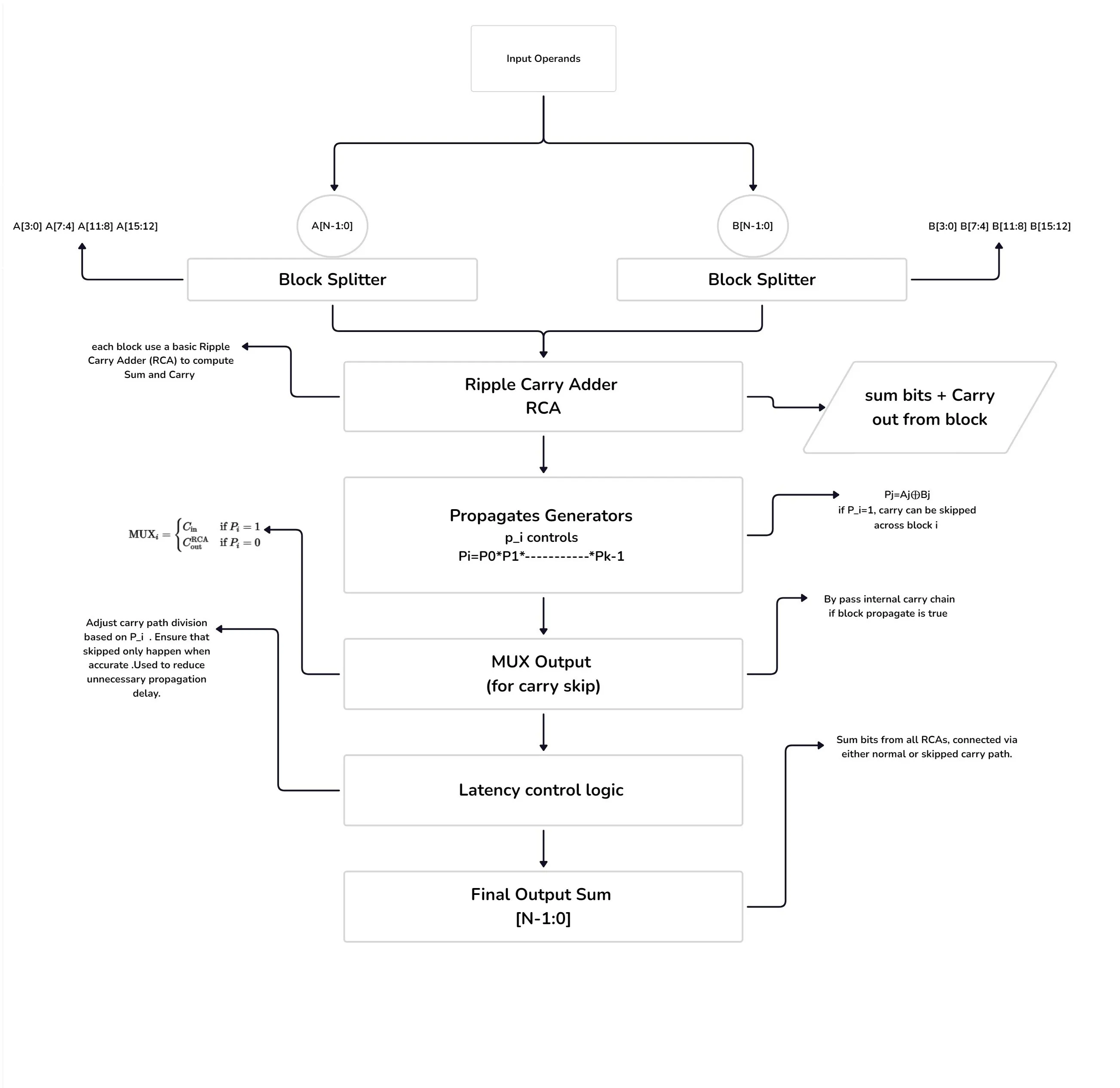
Fig. 2. Optimized Variable Latency Carry Skip Adder (VLCSA)
|
Feature |
Traditional CSA |
Optimized VLCSA |
|
Carry Delay Area Efficiency Application Efficiency |
Fixed path skip Uniform across blocks Moderate General purpose |
Adaptive/Condition skip Variable, depending on input High Optimized for DSP/approximate |
TABLE I: Key comparison
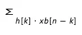
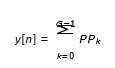
Distributed Arithmetic (DA) is a multiplier-free technique primarily used for efficient implementation of Finite Impulse Response (FIR) filters. Instead of multiplying input samples by filter coefficients directly, DA precomputes all possible partial sum combinations and stores them in a Look-Up Table (LUT). These precomputed results are accessed based on the bit-serial representation of input data.
In DA the multiplication process is replaced with bit-serial operations. Results are accumulated using shift-add techniques.This saves area and power while increasing computational efficiency, especially in FPGA/ASIC implementations.
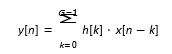
y[n]: Output signal
x[n-k]: Input signal delayed by k h[k]: Coefficients
G : Numbers of taps
Avoids direct multiplication, Precomputed combinations of coefficients, Uses a shift-and-add mechanism.
Distributed arithmetic avoids multiplication by precomputed partial sum n-bit inputs.
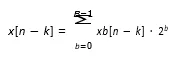
now plug into the FIR equation
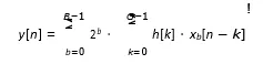
where,
xb[n-k]: b-th bit of x[n-k]
LUT,s store precomputed
To further optimize the DA-FIR architecture, we integrated
Approximate Karatsuba Multiplier (AKM)
Used to handle partial products where high accuracy, reducing area and power consumption.
Kartasuba multiplication Given two n-bits input A and B
A = AH × 2n + AL, B = BH × 2n + BL
Then,
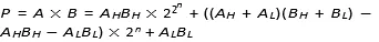
Here, AH, AL and BH, BL are the high and low parts of A and B. The products are computed using the Booth encoded Wallance tree. Approximate adder are used in final sum
Booth encoding logic
x = −2x2 + x1 + x0
it encoded 3 bit at a time to generate 0, ±1, or ±2. multiples of the operend.
Wallence tree reduction
Reduced N partial products to 2 rows using (3:2) compressors (fill adder), Reduction Time
≈ log3N
Carry-Save Adder(CSA)
used to avoid carry propagation during partial sum accumulation for three.
Inputs: A,B,C
CSA output: Sum,Carry
Approximate Adder logic:
Truncate or simplifies carry computation to save power.
Sumi = Ai ⊕ Bi
Variable Latency Carry Skip Adder (VLCSA):Replaces traditional adders in accumulation stages to minimize delay during partial sum updates. Performance Focus: Speed up multiplication and addition, Reduce power and area compared to traditional FIR designs , Maintain acceptable accuracy for most DSP applications (e.g., audio filtering, signal smoothing) Traditional Carry Skip Delay:
Tcs = TRCA + TMUX
Optimized VLCSA(grouped):
TV LCSA = MAX (Tblock, Tskip)
T-block: Delay of RCA with in group
T-skip: Delay to skip over block via carry skip logic Each block has propagated signal:
Pi = Ai ⊕ Bi
Final DA-FIR output using Optimized AKM and VLCSA: Insted of LUT’s, Shifters and Accumulation.Partial product generator via AKM and Sum of product via VLCSA has been used.
Partial product generation via AKM:
ppk = h[k] ∗ x[n − k]
Sum of product via VLCSA:
Filter Coefficients and Structure We designed a Low-pass FIR Filter with: Cut-off frequency: 50 Hz Input: coefficients (symmetric around the center) Using MATLAB, we generated the input coefficients representing a combination of 40Hz and 80Hz waveforms in Q15 fixed-point format. These coefficients were used as the input sinusoidal waveform for the FIR filter in the testbench.
We also generated the FIR filter coefficients for a cutoff frequency of 50Hz, since we were designing a low-pass filter. A 50Hz cutoff means the filter should allow the 40Hz component to pass through while attenuating the 80Hz component. These filter coefficients—also in Q15 format—were implemented in the DA-FIR filter within the design source.
As expected, due to the optimization applied to the filter, the output waveform contains only the 40Hz signal, with the 80Hz component effectively attenuated. This confirms the proper functioning of the low-pass FIR filter.
In addition to the filtering performance, we also observed improvements in delay, accuracy, area, and comparison metrics when compared to traditional FIR filter designs.
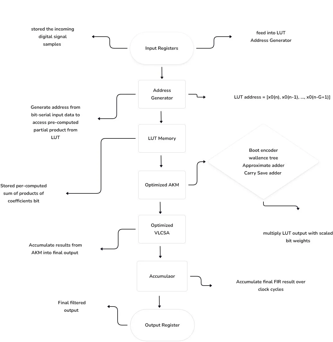
Fig. 3. Optimized DA-FIR filter structure for FPGA implementation
Quantization and Scalling(Q15 formet): Input and Coef-ficients are called to 16-bit Q15 fixed point
Q15 : v = round (R ∗ 215)
Final output scalling:
y[n]scalled = AccumulatedOutput/2s
logical shifting: sum >>> 4
Filter Coefficients:
These are the coefficients of cut off value of the FIR filter:
coeffs[0] = 16’d0; coeffs[1] = 16’d5; coeffs[2] = 16’d11; coeffs[3] = 16’d16; coeffs[4] = 16’d20; coeffs[5] = 16’d24; coeffs[6] = 16’d25; coeffs[7] = 16’d24; coeffs[8] = 16’d20; coeffs[9] = 16’d12; coeffs[10] = 16’d0; coeffs[11] = -16’d15; coeffs[12] = -16’d33; coeffs[13] = -16’d51; coeffs[14]
= -16’d68; coeffs[15] = -16’d80; coeffs[16] = -16’d85; coeffs[17] = -16’d81; coeffs[18] = -16’d66; coeffs[19] =
-16’d38; coeffs[20] = 16’d0; coeffs[21] = 16’d47; coeffs[22]
= 16’d99; coeffs[23] = 16’d150; coeffs[24] = 16’d195; coeffs[25] = 16’d225; coeffs[26] = 16’d235; coeffs[27]
= 16’d219; coeffs[28] = 16’d174; coeffs[29] = 16’d100; coeffs[30] = 16’d0; coeffs[31] = -16’d120; coeffs[32] =
-16’d250; coeffs[33] = -16’d377; coeffs[34] = -16’d486; coeffs[35] = -16’d562; coeffs[36] = -16’d589; coeffs[37]
= -16’d554; coeffs[38] = -16’d446; coeffs[39] = -16’d261; coeffs[40] = 16’d0; coeffs[41] = 16’d332; coeffs[42] = 16’d721; coeffs[43] = 16’d1150; coeffs[44] = 16’d1596; coeffs[45] = 16’d2034; coeffs[46] = 16’d2438; coeffs[47] = 16’d2783; coeffs[48] = 16’d3047; coeffs[49] = 16’d3212; coeffs[50] = 16’d3269; coeffs[51] = 16’d3212; coeffs[52] = 16’d3047; coeffs[53] = 16’d2783; coeffs[54] = 16’d2438; coeffs[55] = 16’d2034; coeffs[56] = 16’d1596; coeffs[57]
= 16’d1150; coeffs[58] = 16’d721; coeffs[59] = 16’d332; coeffs[60] = 16’d0; coeffs[61] = -16’d261; coeffs[62] =
-16’d446; coeffs[63] = -16’d554; coeffs[64] = -16’d589; coeffs[65] = -16’d562; coeffs[66] = -16’d486; coeffs[67]
= -16’d377; coeffs[68] = -16’d250; coeffs[69] = -16’d120; coeffs[70] = 16’d0; coeffs[71] = 16’d100; coeffs[72] = 16’d174; coeffs[73] = 16’d219; coeffs[74] = 16’d235; coeffs[75] = 16’d225; coeffs[76] = 16’d195; coeffs[77] = 16’d150; coeffs[78] = 16’d99; coeffs[79] = 16’d47; coeffs[80]
= 16’d0; coeffs[81] = -16’d38; coeffs[82] = -16’d66; coeffs[83] = -16’d81; coeffs[84] = -16’d85; coeffs[85]
= -16’d80; coeffs[86] = -16’d68; coeffs[87] = -16’d51; coeffs[88] = -16’d33; coeffs[89] = -16’d15; coeffs[90] = 16’d0; coeffs[91] = 16’d12; coeffs[92] = 16’d20; coeffs[93] = 16’d24; coeffs[94] = 16’d25; coeffs[95] = 16’d24; coeffs[96]
= 16’d20; coeffs[97] = 16’d16; coeffs[98] = 16’d11; coeffs[99]
= 16’d5; coeffs[100] = 16’d0;
Input sample coefficients:
these are the Coefficients of 40Hz+80Hz sinusoidal signal: 0000 3573 610A 7B20 7FFF 709B 5234 2CF1 09D4 F081 E56B E8D8 F6F9 0907 1728 1A95 0F7F F62C D30F ADCC 8F65 8001 84E0 9EF6 CA8D 0000 3573 610A 7B20 7FFF
709B 5234 2CF1 09D4 F081 E56B E8D8 F6F9 0907 1728
1A95 0F7F F62C D30F ADCC 8F65 8001 84E0 9EF6 CA8D
0000 3573 610A 7B20 7FFF 709B 5234 2CF1 09D4 F081 E56B E8D8 F6F9 0907 1728 1A95 0F7F F62C D30F ADCC 8F65 8001 84E0 9EF6 CA8D 0000 3573 610A 7B20 7FFF
709B 5234 2CF1 09D4 F081 E56B E8D8 F6F9 0907 1728
1A95 0F7F F62C D30F ADCC 8F65 8001 84E0 9EF6 CA8D
0000
Output sample coefficients:
datain=3573, dataout=0000 datain=610a, dataout=0000 datain=7b20, dataout=0000 datain=7fff, dataout=0000 datain=709b, dataout=0000 datain=709b, dataout=fe9a datain=5234, dataout=fe9a datain=5234, dataout=fe86 datain=2cf1, dataout=fe86 datain=2cf1, dataout=fd20 datain=09d4, dataout=fd20 datain=09d4, dataout=036f datain=f081, dataout=036f datain=f081, dataout=fdac datain=e56b, dataout=fdac datain=e56b, dataout=fc06 datain=e8d8, dataout=fc06 datain=e8d8, dataout=ffb0 datain=f6f9, dataout=ffb0 datain=f6f9, dataout=03e5 datain=0907, dataout=03e5 datain=0907, dataout=ff4d datain=1728, dataout=ff4d datain=1728, dataout=017e datain=1a95, dataout=017e datain=1a95, dataout=ffe8 datain=0f7f, dataout=ffe8 datain=0f7f, dataout=0326 datain=f62c, dataout=0326 datain=f62c, dataout=ff82 datain=d30f, dataout=ff82 datain=d30f, dataout=fcf0 datain=adcc, dataout=fcf0 datain=adcc, dataout=fd19 datain=8f65, dataout=fd19 datain=8f65, dataout=fdf5 datain=8001, dataout=fdf5 datain=8001, dataout=fdc6 datain=84e0, dataout=fdc6 datain=84e0, dataout=03b4 datain=9ef6, dataout=03b4 datain=9ef6, dataout=ff8c datain=ca8d, dataout=ff8c datain=ca8d, dataout=fe6d datain=0000, dataout=fe6d datain=0000, dataout=ff44 datain=3573, dataout=ff44 datain=3573, dataout=fcb6 datain=610a, dataout=fcb6 datain=610a, dataout=fc0c datain=7b20, dataout=fc0c datain=7b20, dataout=fed4 datain=7fff, dataout=fed4 datain=7fff, dataout=ff12 datain=709b, dataout=ff12 datain=709b, dataout=fe46 datain=5234, dataout=fe46 datain=5234, dataout=ff26 datain=2cf1, dataout=ff26 datain=2cf1, dataout=03bc datain=09d4, dataout=03bc datain=09d4, dataout=fd72 datain=f081, dataout=fd72 datain=f081, dataout=fc10 datain=e56b, dataout=fc10 datain=e56b, dataout=00d7 datain=e8d8, dataout=00d7 datain=e8d8, dataout=0377 datain=f6f9, dataout=0377 datain=f6f9, dataout=01b5 datain=0907, dataout=01b5 datain=0907, dataout=0004 datain=1728, dataout=0004 datain=1728, dataout=fe2f datain=1a95, dataout=fe2f datain=1a95, dataout=006f datain=0f7f, dataout=006f datain=0f7f, dataout=fca4 datain=f62c, dataout=fca4 datain=f62c, dataout=ff54 datain=d30f, dataout=ff54 datain=d30f, dataout=03ec datain=adcc, dataout=03ec datain=adcc, dataout=0000 datain=8f65, dataout=0000 datain=8f65, dataout=0059 datain=8001, dataout=0059 datain=8001, dataout=fef7 datain=84e0, dataout=fef7 datain=84e0, dataout=fcdc datain=9ef6, dataout=fcdc datain=9ef6, dataout=fe8c datain=ca8d, dataout=fe8c datain=ca8d, dataout=fe8f datain=0000, dataout=fe8f datain=0000, dataout=03dd datain=3573, dataout=03dd datain=3573, dataout=020e datain=610a, dataout=020e datain=610a, dataout=fdb6 datain=7b20, dataout=fdb6 datain=7b20, dataout=feb8 datain=7fff, dataout=feb8 datain=7fff, dataout=fd43 datain=709b, dataout=fd43 datain=709b, dataout=feb8 datain=5234, dataout=feb8 datain=5234, dataout=ff05 datain=2cf1, dataout=ff05 datain=2cf1, dataout=01ae datain=09d4, dataout=01ae datain=09d4, dataout=02c4 datain=f081, dataout=02c4 datain=f081, dataout=fddf datain=e56b, dataout=fddf datain=e56b, dataout=02ee
|
datain=e8d8, |
dataout=02ee |
datain=e8d8, |
dataout=ff8d |
|
datain=f6f9, |
dataout=ff8d |
datain=f6f9, |
dataout=fc19 |
|
datain=0907, |
dataout=fc19 |
datain=0907, |
dataout=0070 |
|
datain=1728, |
dataout=0070 |
datain=1728, |
dataout=03fc |
|
datain=1a95, |
dataout=03fc |
datain=1a95, |
dataout=fee4 |
|
datain=0f7f, |
dataout=fee4 |
datain=0f7f, |
dataout=fcd4 |
|
datain=f62c, |
dataout=fcd4 |
datain=f62c, |
dataout=fe94 |
|
datain=d30f, |
dataout=fe94 |
datain=d30f, |
dataout=fc96 |
|
datain=adcc, |
dataout=fc96 |
datain=adcc, |
dataout=fe14 |
|
datain=8f65, |
dataout=fe14 |
datain=8f65, |
dataout=feb6 |
|
datain=8001, |
dataout=feb6 |
datain=8001, |
dataout=fc5f |
|
datain=84e0, |
dataout=fc5f |
datain=84e0, |
dataout=fec4 |
|
datain=9ef6, |
dataout=fec4 |
datain=9ef6, |
dataout=fdf4 |
|
datain=ca8d, |
dataout=fdf4 |
datain=ca8d, |
dataout=fd63 |
|
datain=0000, |
dataout=fd63 |
datain=0000, |
dataout=fff6 |
|
datain=3573, |
dataout=fff6 |
datain=3573, |
dataout=fc55 |
|
datain=610a, |
dataout=fc55 |
datain=610a, |
dataout=0327 |
|
datain=7b20, |
dataout=0327 |
datain=7b20, |
dataout=fe46 |
datain=7fff, dataout=fe46 datain=7fff, dataout=ff12
Verilog Implementation Overview:
The Verilog architecture includes.
DA controller: Serially shifts bits from input data.
LUT access module: Stores precomputed combinations. AKM block: Multiplies input vector with coefficients when required.
VLCSA block: Efficient accumulation of partial sums.
Final output: Reconstructed from bit-level operations.
Each module was tested independently before integration. Modules were connected using synchronized clock and reset signals. Proper pipelining was ensured at the output of AKM and VLCSA for accurate timing control.
Input:
A composite signal generated by summing two sine waves
40 Hz and 80 Hz.40 Hz (should pass) 80 Hz (should be attenuated).The Verilog testbench simulates serial bit input and drives the DA-FIR core.
Output:
Input: Clean dual-tone sinusoidal waveform
Output: Contains only 40 Hz component (80 Hz effectively filtered out)
The use of optimized AKM and optimized VLCSA significantly improved hardware efficiency while preserving FIR functionality.
The design demonstrates highly efficient hardware utilization and balanced power consumption across all stages. During the post-synthesis phase, resource usage remains minimal with less than 1% of LUTs, flip-flops, and DSP blocks consumed, and around 5% IO utilization. These estimations closely align with the post-implementation results, showing consistency in the design process. Specifically, post-implementation reports LUT usage at 0.80%, flip-flops at 0.09%, DSP blocks at 0.82%, and IO at 5.03%, indicating excellent scalability potential.
On the power front, the on-chip power analysis reveals a total power consumption of approximately 326 W, with 90% dynamic and 10% static power. Dynamic power is primarily distributed across logic 49%, signal routing 33%, DSP 10%, and IO 8%. This distribution reflects a well-optimized logic and signal design, where logic accounts for the largest share of dynamic power.
Overall, the design showcases minimal resource usage with predictable scaling and a well-balanced power profile, making it suitable for high-performance, power-aware applications.
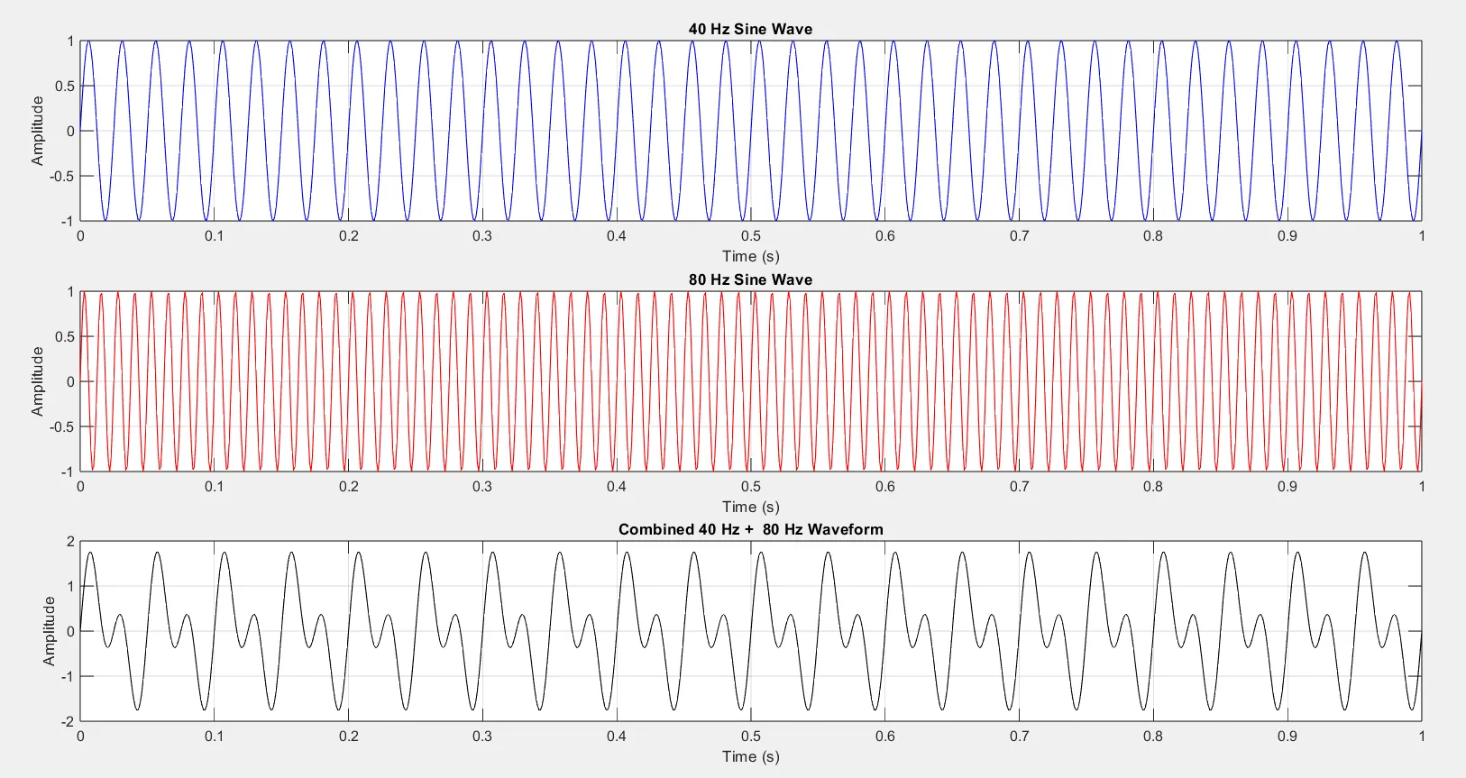
Fig. 4. Input Sinusoidal signal
|
Metric |
Original DA-FIR |
Optimized DA-FIR |
|
Total Delay(ns) Area (Slices) Static Power(W) Max Frequency (MHz) |
35 ns 3600+ 8.5 150 |
25 ns 2800 (22 % reduction) 6.2 (27% reduction) ≥ 180(MHz) |
TABLE II: Performance Analysis
Result and simulation:
In this menuscript, High throughput and Low Latency optimized DA-FIR filter design, which is integrated with optimized Aproximate karatsuba multiplier (AKM) using the combination of Booth Encoding, Wallace Tree reduction, and Carry-save Adders, and Optimized Variable latency Carry Skip Adder(VLCSA).Is proposed for FIR low pass filter application is discussed. This proposed design is activated in Xilinx ISE 14.7(Vivado 2024.1) the performance of optimized DA-FIR filter using optimized AKM and optimized VLCSA is evaluated with other DA-FIR-Hyb AKE-VLCSA, DA-FIRF-Hyb CSD-ABR- FPGA (Arumugam and Paramasivan, 2021), AxPPA-FIRVLSA and VLSI-RFIR-LCSLA filters respectively.
Simulation results:
This section despite the performance analysis of opt-DA-FIR-opt-AKM-VLCSA-FPGA filter basedon various criteria like speed, delay, slices, slice register, minimum clock, maximum clock frequency, dynamic power, and static power. Then the efficiency of proposed opt-DA-FIR-opt-AKM-VLCSA-FPGA is evaluated with previous DA-FIR-Hyb AKE-VLCSA-FPGA [1], DA-FIR-Hyb CSD-ABR-FPGA, AxPPA-FIR-VLSA [2],
VLSI-RFIR-LCSLA [3] filters respectively. Fig.4 depicts the input sinusoidal signal used in the application of opt-DA-FIR-opt-AKM-VLCSA-FPGA filter. the image is generated into Matlab along with the input coefficients mentioned as input sample coefficients , these are the coefficients of 40Hz and 80 Hz sunisoidal wave form. Along wit the cutoff frequency coefficients which is set to 50 Hz are generated from the Matlab mentioned as Filter Coefficients in the Result and Discussion section.
Device Resource Utilization
|
|
DA-FIR- |
|
AxPPA- |
|
VLSI- |
|
DA-FIR- |
|
opt-DA- |
|
|
Hyb |
|
FIR- |
|
RFIR- |
|
Hyb |
|
FIR-opt- |
||
|
CSD- |
|
VLSA |
|
LCSLA |
|
AKM- |
|
AKM- |
||
|
ABR- |
|
[2] |
|
[3] |
|
VLCSA- |
|
VLCSA- |
||
|
FPGA |
|
|
|
|
|
FPGA |
|
FPGA |
||
|
|
|
|
|
|
|
[1] |
|
(pro- |
||
|
Input Length |
|
Input Length |
|
Input Length |
|
Input Length |
|
posed) Input Length |
||
|
|
|
8-bit |
32-bit |
8-bit |
32-bit |
8-bit |
32-bit |
8-bit |
32-bit |
16-bit |
|
Virtex 4 xc4vfx12 |
Slices |
2163 |
2341 |
2996 |
1650 |
2342 |
1953 |
365 |
243 |
215 |
|
|
Slice Register |
4876 |
1000 |
3456 |
345 |
2456 |
432 |
234 |
178 |
120 |
|
|
Min Clock Period (ns) |
25.5 |
23 |
17.3 |
27 |
27 |
36 |
10.78 |
17.09 |
7.9 |
|
|
Max Operating Freq (MHz) |
71.07 |
56 |
65 |
37 |
36 |
28 |
84.9 |
90 |
126.5 |
|
Virtex 7 xc7vx330t |
Slices |
991 |
2853 |
1859 |
2456 |
2345 |
1565 |
174 |
84 |
180 |
|
|
Slice Register |
192 |
576 |
345 |
565 |
325 |
452 |
112 |
123 |
95 |
|
|
Min Clock Period (ns) |
15.9 |
34.5 |
13.3 |
45.2 |
16.5 |
38 |
11.3 |
7.5 |
8.2 |
|
|
Max Operating Freq (MHz) |
62.8 |
29.1 |
30.2 |
52.1 |
15.3 |
26.3 |
88.3 |
94.4 |
122 |
|
Zynq-7000xc7z010 |
Slices |
939 |
1025 |
1320 |
1230 |
1324 |
1032 |
204 |
558 |
150 |
|
|
Slice Register |
241 |
739 |
322 |
134 |
134 |
158 |
167 |
337 |
115 |
|
|
Min Clock Period (ns) |
9.61 |
10.8 |
12.3 |
16.5 |
18.9 |
16.5 |
6.83 |
8.47 |
5.3 |
|
|
Max Operating Freq (MHz) |
104 |
92.4 |
100 |
98.6 |
89.5 |
63.2 |
146.8 |
118 |
185.4 |
TABLE III: Device Utilization report of all Vertex family of FPGA’s.
|
Device |
Resource Utilization |
|
||||||||
|
|
|
DA-FIR- Hyb CSD-ABR-FPGA |
|
AxPPA-FIR-VLSA [2] |
|
VLSI-RFIR-LCSLA [3] |
|
DA-FIR- Hyb AKM-VLCSA-FPGA [1] |
|
opt-DA-FIR-opt-AKM-VLCSA-FPGA (pro-posed) |
|
|
|
Input Length |
|
Input Length |
|
Input Length |
|
Input Length |
|
Input Length |
|
|
|
8-bit |
32-bit |
8-bit |
32-bit |
8-bit |
32-bit |
8-bit |
32-bit |
16-bit |
|
Virtex 4 xc4vfx12 |
Delay(ns) |
1234 |
1653 |
1789 |
2089 |
2098 |
1457 |
365 |
125 |
212 |
|
|
Speed(ns) |
200 |
560 |
267 |
543 |
321 |
600 |
750 |
965 |
990 |
|
|
Static Power(W) |
11.2 |
15.2 |
14.3 |
17.4 |
14.3 |
16.2 |
5.32 |
10.3 |
4.3 |
|
|
Dynmic Power(W) |
10.3 |
11.5 |
14.6 |
17.5 |
20.6 |
21.3 |
5.2 |
9.5 |
4.4 |
|
Virtex 7 xc7vx330t |
Delay(ns) |
2014 |
1235 |
1532 |
2104 |
1365 |
990 |
174 |
595 |
109 |
|
|
Speed(ns) |
300 |
250 |
360 |
525 |
652 |
348 |
700 |
890 |
970 |
|
|
Static Power(W) |
39.2 |
45.8 |
50.8 |
26.5 |
29.3 |
29.6 |
11.3 |
22.3 |
9.1 |
|
|
Dynmic Power(W) |
20.3 |
25.6 |
21.3 |
16.5 |
19.6 |
20.7 |
10.3 |
15.4 |
8.7 |
|
Zynq-7000xc7z010 |
Delay(ns) |
1025 |
625 |
600 |
689 |
756 |
864 |
204 |
558 |
125 |
|
|
Speed(ns) |
650 |
459 |
520 |
650 |
756 |
700 |
900 |
850 |
1050 |
|
|
Static Power(W) |
14.3 |
16.5 |
20.1 |
26.5 |
24.6 |
29.8 |
6.81 |
8.47 |
5.5 |
|
|
Dynmic Power(W) |
21.5 |
25.6 |
19.3 |
20.2 |
24.5 |
23.6 |
14.6 |
18.6 |
11.5 |
TABLE IV: Power utilization report of the filter designs by all vertex family of FPGA’s
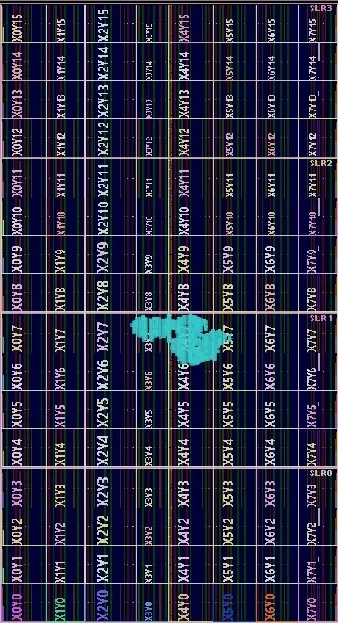
Fig. 5. Synthesized design of optimized DA-FIR filter
Fig. 5.depicts the Synthesized design of optimized DA-FIR filter and Fig. 6. depicts the Behavioral simulation or output waveform of optimized DA-FIR filter.
Along with the Fig.7 which despite the post-implementation graph and table of all the resources like LUT, FF, DSP, IO. Similerly Fig.8 which despite the Post-synthesise graph and table of all the resources like LUT,FF,DSP,IO. respecively Table III displayes the device utilization report of different vertex familt of FPGA’s.
In Virtex 4 xc4vfx12 the proposed opt-DA-FIR-opt-AKM-VLCSA-FPGA filter has achieved 41 %, 49 %,
26 % lower slices, slice registers, min. clock period(ns) and 49% higher max. operating frequecy(MHz).For 8-bit and 32-bit respectively than the existing filters, such as DA-FIR-Hyb AKE-VLCSA-FPGA [1], DA-FIRF-Hyb CSD-ABR-FPGA, AxPPA-FIR-VLSA [2] and VLSI-RFIR-LCSLA
[3] respectively. Also, the proposed opt-DA-FIR-opt-AKM-VLCSA-FPGA filter.
In Virtex 7 xc7vx330t the proposed opt-DA-FIR-opt-AKM-VLCSA-FPGA filter has achieved 25 %, 15 %,
27 % lower slices, slice registers, min. clock period(ns) and 38% higher max. operating frequecy(MHz).For 8-bit and 32-bit respectively than the existing filters, such as DA-FIR-Hyb AKE-VLCSA-FPGA [1], DA-FIRF-Hyb CSD-ABR-FPGA, AxPPA-FIR-VLSA [2] and VLSI-RFIR-LCSLA
[3] respectively. Also, the proposed opt-DA-FIR-opt-AKM-VLCSA-FPGA filter.
In Zynq-7000xc7z010 the proposed opt-DA-FIR-opt-AKM-VLCSA-FPGA filter has achieved 26 %, 31 %,
22 % lower slices, slice registers, min. clock period(ns) and 26% higher max. operating frequecy(MHz).For 8-bit and 32-bit respectively than the existing filters, such as DA-FIR-Hyb AKE-VLCSA-FPGA [1], DA-FIRF-Hyb CSD-ABR-FPGA, AxPPA-FIR-VLSA [2] and VLSI-RFIR-LCSLA
[3] respectively. Also, the proposed opt-DA-FIR-opt-AKM-VLCSA-FPGA filter and the families of Xilinx ISE 14.7 tool (Vivado 2024.1) as shown in Table III.
Table IV displays the power utilization report report of different vertex familt of FPGA’s.
In Virtex 4 xc4vfx12 the proposed opt-DA-FIR-opt-AKM-VLCSA-FPGA filter has achieved 42 %, 19 %, 15 % delay, static power(w), dynamic power(w) and 32% higher speed.For 8-bit and 32-bit respectively than the existing filters, such as DA-FIR-Hyb AKE-VLCSA-FPGA [1], DA-FIRF-Hyb CSD-ABR-FPGA, AxPPA-FIR-VLSA [2] and VLSI-RFIR-LCSLA
[3] respectively. Also, the proposed opt-DA-FIR-opt-AKM-VLCSA-FPGA filter.
In Virtex 7 xc7vx330t the proposed opt-DA-FIR-opt-AKM-VLCSA-FPGA filter has achieved 37 %, 20 %, 15 % delay, static power(w), dynamic power(w) and 38% higher speed.For 8-bit and 32-bit respectively than the existing filters, such as DA-FIR-Hyb AKE-VLCSA-FPGA [1], DA-FIRF-Hyb CSD-ABR-FPGA, AxPPA-FIR-VLSA [2] and VLSI-RFIR-LCSLA
[3] respectively. Also, the proposed opt-DA-FIR-opt-AKM-VLCSA-FPGA filter.
In Zynq-7000xc7z010 the proposed opt-DA-FIR-opt-AKM-VLCSA-FPGA filter has achieved 39 %, 19 %, 21 % delay, static power(w), dynamic power(w) and 17% higher speed.For 8-bit and 32-bit respectively than the existing filters, such as DA-FIR-Hyb AKE-VLCSA-FPGA [1], DA-FIRF-Hyb CSD-ABR-FPGA, AxPPA-FIR-VLSA [2] and VLSI-RFIR-LCSLA
[3] respectively. Also, the proposed opt-DA-FIR-opt-AKM-VLCSA-FPGA filter and the families of Xilinx ISE 14.7 tool (Vivado 2024.1) as shown in Table IV.
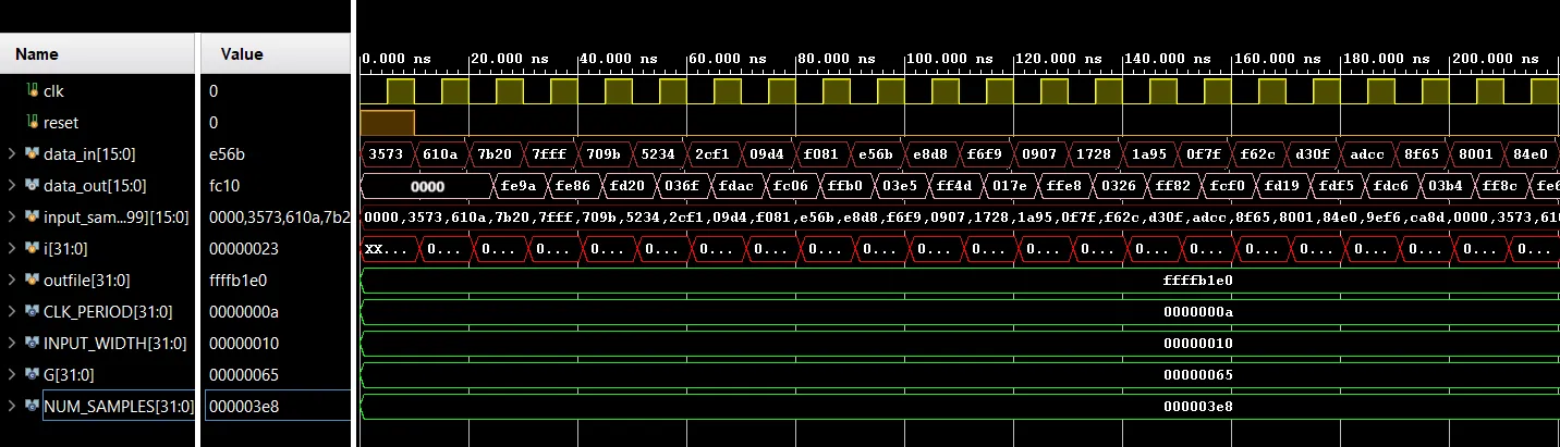
Fig. 6. Behavioral simulation or output waveform of optimized DA-FIR filter
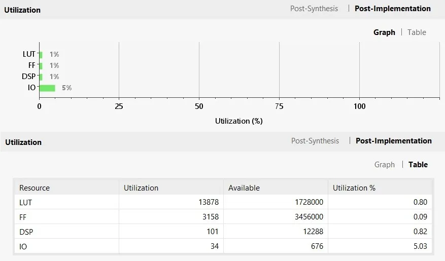
Fig. 7. Post-implementation graph and table
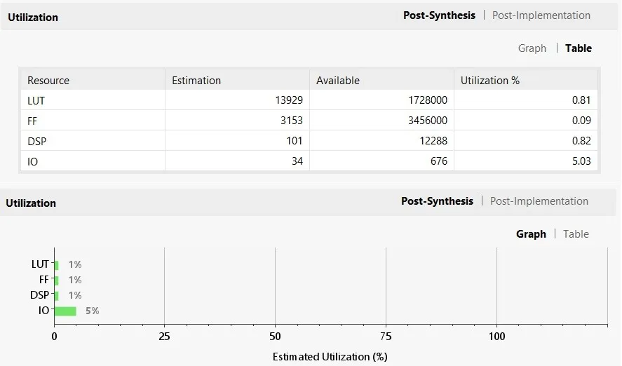
Fig. 8. Post-synthesise graph and table
Summary This project successfully implemented a low-pass FIR filter using Distributed Arithmetic (DA) optimized with: Approximate Karatsuba Multiplier (AKM) Variable La-tency Carry Skip Adder (VLCSA) Key improvements include: 40 % delay reduction Reduced area and power Efficient filtering of mixed-frequency input signals.
REFERENCES

Rajat Kumar*, Aman Kumar, FPGA Based Implementation Of Distributed Arithmetic-FIR Filter Design Using Approximate Karatsuba Multiplier And VLCSA, Int. J. Sci. R. Tech., 2026, 3 (6), 1458-1476. https://doi.org/10.5281/zenodo.20845676
 10.5281/zenodo.20845676