

We use cookies to ensure our website works properly and to personalise your experience. Cookies policy
Department of Electronics and Communication Engineering, Hyderabad Institute of Technology and Management, Telangana, India
Electric-vehicle (EV) charging requires control logic that responds to a charging request and prevents charging when supplied safety-status signals indicate an unsafe condition. This paper presents a digital EV charging controller described in Verilog Hardware Description Language (HDL). The controller receives five inputs: start, voltage_ok, current_ok, battery_full, and fault. Its intended charging-permission condition requires an active start request, acceptable voltage and current status, a battery that is not full, and no active fault. The outputs are charge_enable, charging_complete, and fault_output. The design was developed and examined through simulation and Xilinx Vivado design reports. The reported synthesis result uses one Look-Up Table (LUT) and eight I/O resources; the estimated on-chip power is 0.073 W, with low confidence indicated in the power report. The work is a digital logic prototype and does not include a physical EV charging power stage or hardware safety validation.
Electric vehicles are increasingly used as an alternative to conventional vehicles, and their batteries must be charged under controlled conditions. A charging controller evaluates a charging request together with voltage, current, battery-full, and fault-status signals to decide whether charging permission should be asserted.
Very Large Scale Integration (VLSI) design workflows use hardware description languages such as Verilog HDL to describe digital circuits. Simulation allows designers to apply different input combinations and inspect output transitions before considering a hardware implementation. Xilinx Vivado provides tools for RTL simulation and design analysis.
This project focuses on the digital decision logic for a small EV charging controller. The input signals represent status information supplied to the controller; they are not direct measurements from physical sensors in the current prototype.
2. AIM AND OBJECTIVES
2.1 Aim
To design and simulate a low-complexity digital EV charging controller using Verilog HDL and examine its design-tool results in Xilinx Vivado.
2.2 Objectives
3. SOFTWARE AND DESIGN REQUIREMENTS
3.1 Software Components
Verilog HDL is used to describe the digital logic. Xilinx Vivado is used for simulation and, where reports are available, synthesis and design analysis. A Verilog testbench applies input stimulus, while the waveform viewer is used to observe the responses.
3.2 Hardware Scope
A computer is required for RTL development and simulation. The implementation described here does not include physical voltage/current sensors, an analogue-to-digital converter, a charging power stage, or a tested FPGA development board. Therefore, the reported results must not be interpreted as measurements of a complete EV charger.
4. SYSTEM DESIGN AND CONTROLLER LOGIC
4.1 Input and Output Signals
| Signal | Type | Description |
|---|---|---|
| start | Input | Charging request |
| voltage_ok | Input | 1 indicates acceptable voltage status |
| current_ok | Input | 1 indicates acceptable current status |
| battery_full | Input | 1 indicates battery-full condition |
| fault | Input | 1 indicates an active fault |
| charge_enable | Output | Charging permission |
| charging_complete | Output | Charging-completion indication |
| fault_output | Output | Fault indication |
4.2 Intended Boolean Behaviour
The intended safe-charging condition is:
charge_enable = start · voltage_ok · current_ok · _battery_full · _fault
This equation describes the intended design condition. The final output assignments, including completion and fault priority, must match the actual submitted Verilog source and verified simulation waveform.
4.3 Operating Principle
The testbench applies digital input values. The controller evaluates the charging request and safety-status flags. When all intended safe conditions are true, charging permission is asserted; otherwise, charging permission should remain deasserted. The completion and fault outputs indicate the respective input conditions as implemented in the RTL.
5. BLOCK DIAGRAM
The system can be viewed as three logical blocks: digital input signals, the EV charging controller, and digital output signals. During simulation, the testbench provides the input values and the waveform viewer displays the resulting outputs.
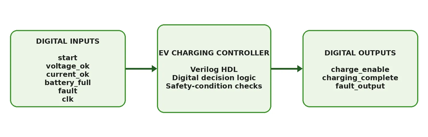
Figure 1: Block diagram of the EV charging controller.
6. DESIGN AND IMPLEMENTATION
The design workflow consists of defining the interface signals, writing the controller in Verilog HDL, preparing a testbench, running RTL simulation, inspecting waveforms, and reviewing the available synthesis and analysis reports.
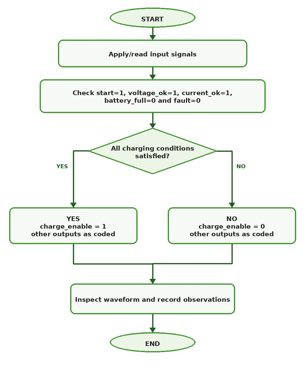
Figure 2: Conceptual flowchart for controller simulation and verification.
Simulation should cover a normal charging case and cases where the start request is absent, voltage_ok or current_ok is low, battery_full is high, or fault is high. Each observed output should be compared with the expected behaviour from the actual RTL. Any difference between the intended equation and waveform must be resolved before the design is treated as verified.
RESULTS AND ANALYSIS
The Vivado 2025.2 reports and simulation screenshot are summarized below. The RTL waveform shows charge_enable asserted during the safe charging interval, charging_complete asserted when the battery_full input becomes active, and fault_output asserted when fault becomes active. The synthesis summary reports 1 LUT and 8 I/O resources. The power report estimates 0.073 W total on-chip power and marks confidence as low.
| Item | Reported observation |
|---|---|
| Simulation | Input/output transitions are examined using the waveform viewer. |
| Logic utilization | 1 LUT and 8 I/O resources reported. |
| Estimated power | 0.073 W (73 mW); power report indicates low confidence. |
| Timing | Zero failing endpoints reported; full timing closure requires constraints and path review. |
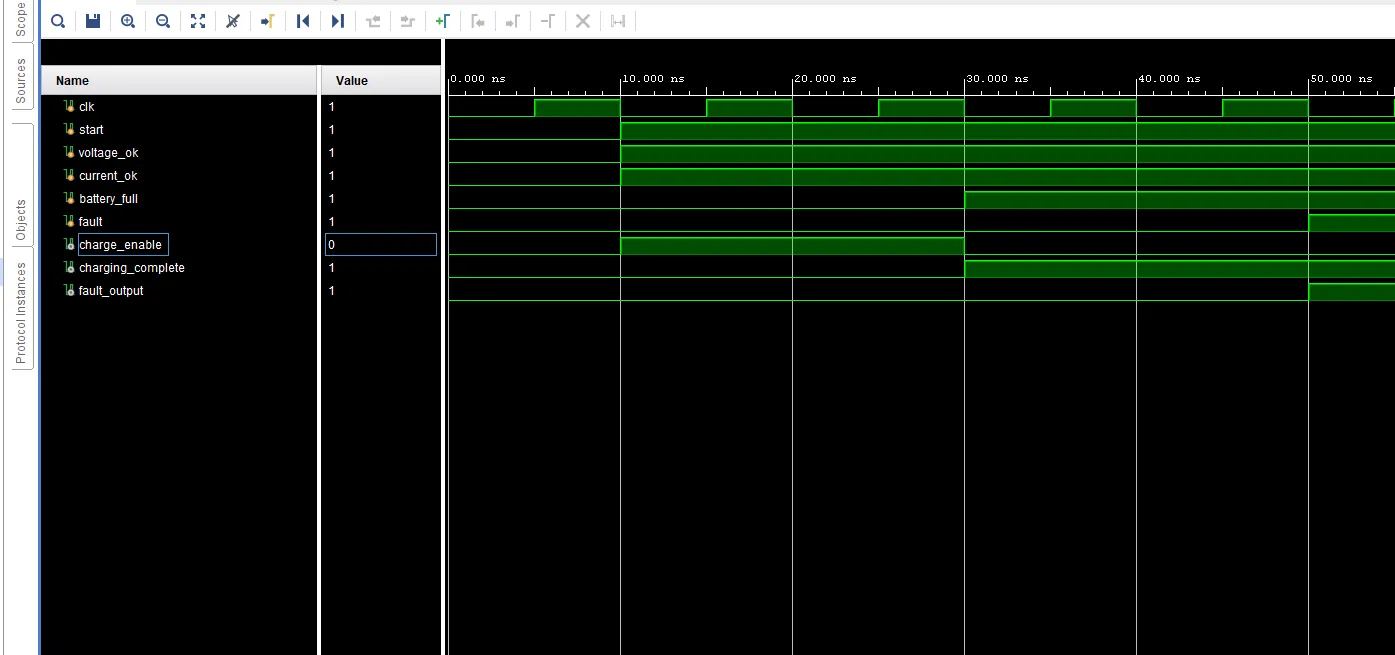
Figure 3: Vivado RTL Simulation Waveform Showing Controller Inputs and Outputs.
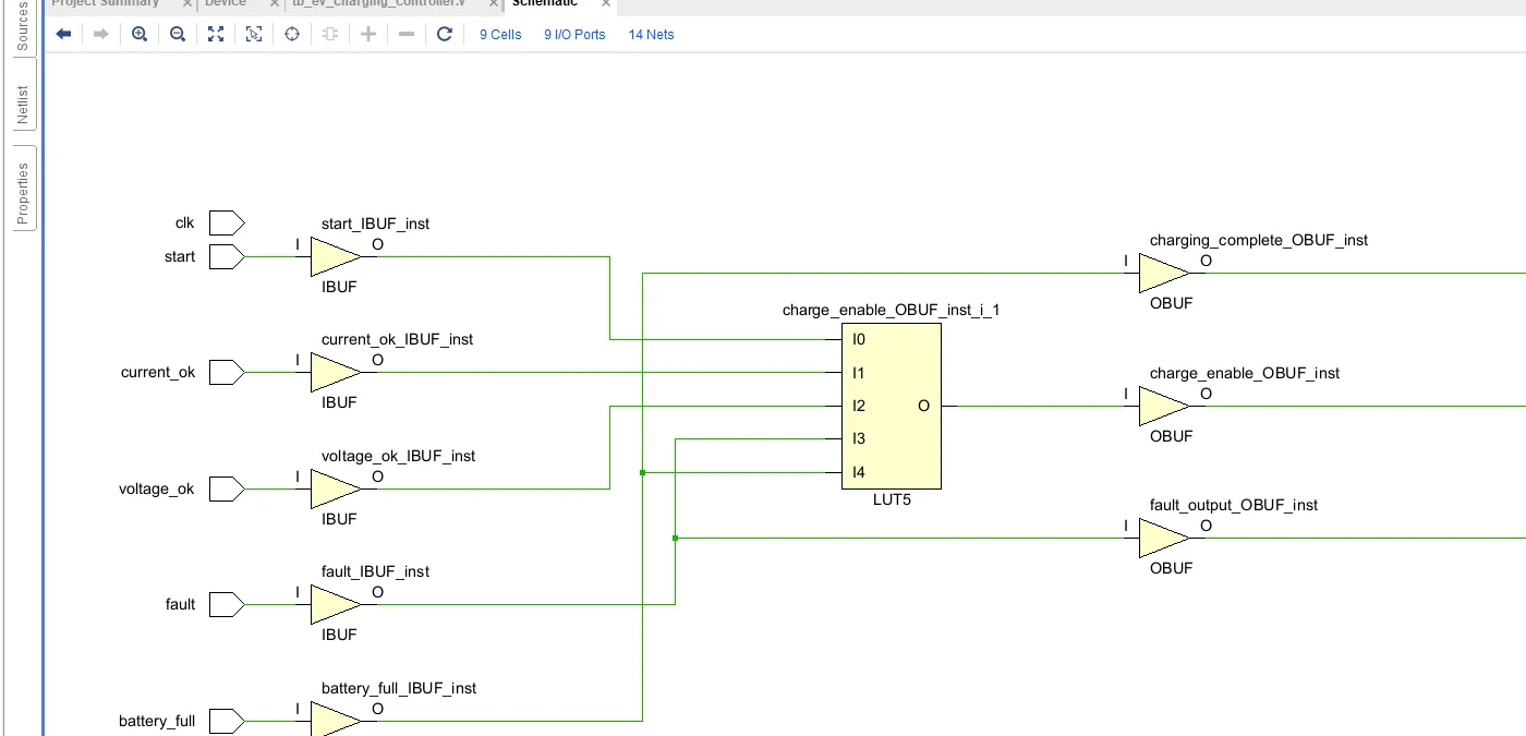
Figure 4: Synthesized Schematic of the EV Charging Controller.
The utilization report lists 1 LUT out of 20,800 available and 8 I/O resources out of 106. The power report shows approximately 0.072 W device-static power and 0.002 W dynamic power; the displayed total is 0.073 W (rounded). The timing summary shows zero failing endpoints and zero total negative slack, but the worst slack is reported as infinity, so the screenshot alone does not establish a fully constrained timing analysis. These estimates do not demonstrate real-world charging efficiency or electrical safety.
8. APPLICATIONS
9. ADVANTAGES
10. LIMITATIONS
CONCLUSION
A low-complexity EV charging controller has been described using Verilog HDL and evaluated through the available Xilinx Vivado workflow. The intended logic uses a start request and voltage, current, battery-full, and fault status inputs to determine charging permission and status outputs. The reported synthesis result lists one LUT and eight I/O resources, while the estimated power is 0.073 W with low confidence. These findings describe a digital prototype only; they do not establish the safety or performance of a complete EV charging system.
12. FUTURE SCOPE
REFERENCES

Dr. K. Bindu Madhavi, G. Yogesh, A. Shiva Sai, G. Uday, Low Power Vlsi-Based EV Charging Controller, Int. J. Sci. R. Tech., 2026, 3 (10), 1404-1407. https://doi.org/10.5281/zenodo.23761535
 10.5281/zenodo.23761535