

We use cookies to ensure our website works properly and to personalise your experience. Cookies policy
1Electronics and Communication Engineering, Srinivasa University Mangalore and LTTS Bangalore.
2Electronics and communication Engineering, Srinivasa University Mangalore.
3NMAM Institute of Technology (NMAMIT), Department of Advanced Communication Technology, Nitte, Karkala, India.
This paper presents a novel framework for low-power ASIC and VLSI physical design with an emphasis on chiplet-based architectures. The proposed system integrates AI interactive visualization interfaces with advanced physical design methodologies to address key challenges across multiple technology nodes. The framework includes tools for AI timing violation heatmap generation, routing congestion analysis, AI macro placement visualization, and power planning isolation, enabling designers to optimize Performance, Power, and Area (PPA) metrics efficiently. Furthermore, the system supports comparative analysis between traditional System-on-Chip (SoC) flows and AI chiplet-based integration, facilitating informed architectural decisions and AI data design trade-offs. The proposed approach significantly reduces design iterations, improves power delivery, and accelerates signoff for next-generation semiconductor AI devices.
Physical design is a critical phase in the integrated circuit (IC) design process, responsible for transforming a circuit's logical description into a layout that can be fabricated on a silicon wafer. This intricate process involves a multitude of inputs that guide the creation of a layout that meets performance, power, and area requirements while adhering to design rules and constraints. In the realm of semiconductor technology, where the pace of miniaturization continues to astonish, the concept of Very Large-Scale Integration (VLSI) has revolutionized the way we perceive electronic devices. At the heart of VLSI lies the intricate process of physical design, a crucial step that transforms logical circuit representations into tangible semiconductor chips. This article delves into the significance of different prerequisites of physical design in VLSI, highlighting its multifaceted importance and the intricacies of the process.
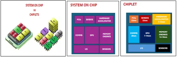
Fig1: Soc v/s chiplet
SoC, System on Chip, is a system-level single chip, which is a combination of multiple computing units responsible for different types of computing tasks, which are fabricated on the same wafer through photolithography
In contrast to SoC, Chiplet is a complex SoC chip that is decomposed into different computing units or functional units at the beginning of the design, and then each unit is manufactured separately using the most suitable semiconductor process technology, and then the various units are interconnected through advanced packaging technology and finally integrated and packaged into a system-level chipset.
ASIC design flow is a set of steps that takes a logical level design into a physically working chip. ASIC design flow is silicon aware design process that is widely used to produce the various semiconductor chips. The ASIC flow starts with specifications where the target design requirements, operating parameters, constraints and models of the design will be developed. This design is coded using hardware description languages (HDLs) (like Verilog, vhdl and system verilog).
The HDL produces a register transfer level (RTL) of the design. This RTL is verified for its functionality by various verification techniques and down streamed for synthesis. The synthesis step converts the RTL to a gate-level netlist. It is the step where the design is mapped to the technology-based cells. The physical design of the block starts with floorplanning where the given area to the block is planned for the various steps in the physical design. The floorplanning steps follow the power planning, where the global distribution of VDD and VSS for each cell in the design is planned. The placement and routing steps places and route all the standard cells (instances) of the design.
RELATED WORK
RELATED WORKS Buffered clock trees are often desirable, but added at the expense of complicating the clock design. From [1], skew due to buffer mismatch is minimized by first clustering the clock nodes so that identical buffers can be used at a level, and balancing the higher-order loads of the clusters so that load dependent buffer delays are matched. Interconnect delays within clusters are concurrently balanced too, thereby generating a low-skew buffered clock tree design. While the two techniques we have presented are most effective when used concurrently, they are completely independent of each other. The clustering technique can be used to generate clusters of equal capacitive loading for any clock tree synthesis methodology.
Similarly, the delay- and admittance-matching wire sizing technique can be used for constructing any buffered clock tree that uses equally-sized buffers at the same level. Crosstalk is a well–known phenomenon at all levels of electronic packaging from system level cables through wires on printed circuit boards and multi–chip–modules to chip level routing. It is an effect due to coupling capacitances and inductances between currents in electrical conductors. Crosstalk causes undesired signal noise to be coupled from an active line (aggressor) into a quiet line (victim). Depending on its magnitude, the induced noise onto the victim may influence the timing be
PROPOSED WORK
The present invention concerns systems, AI methods and visualization AI interfaces through low power ASIC and VLSI physical design with an emphasis on chiplet architecture. The present invention provides an integrated methodology to analyze and tackle physical design challenges across multiple technology nodes starting with the creation of timing violation heatmap displays, routing congestion display devices, macro placements visual devices and power-planning isolation interfaces. The invention also offers a method to support comparative design flows between SoC compliant physical design versus chiplet based integration, which ultimately enables the design to focus on the design of the performance, power and area (PPA) deliverables at advanced technology nodes. By combining physical design methodologies with interactive visualization, the physical design process can significantly skip iterating a debug session, improve power delivery effectiveness, and expediting the implementation of a signoff plan for the next-generation advanced semiconductor devices.
This paper discusses strategies for optimizing the physical design flow of semiconductor chips, particularly at lower technology nodes, to achieve faster turnaround times (TAT) and improved power, performance, and area (PPA) metrics.
Physical Design Flow Overview
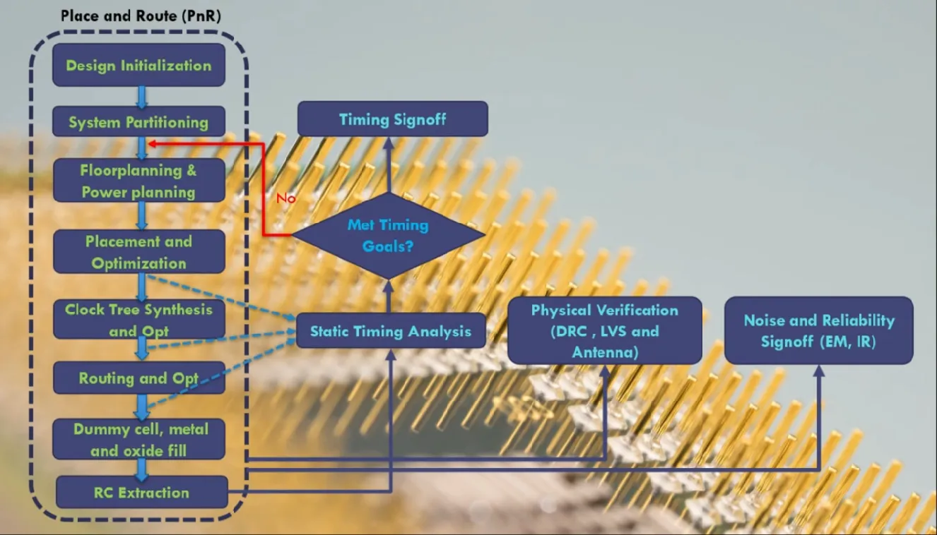
Fig1:AI based physical design flow
The physical design process transforms a logical gate-level netlist into a physical layout suitable for fabrication, involving steps such as floorplanning, power planning, placement, clock tree synthesis (CTS), and routing.
Key Steps in Physical Design
DESIGN PLANNING
Design planning in physical design involves systematically organizing and strategizing the placement and routing of electronic components on a chip to optimize performance, power consumption, and manufacturability. It includes defining the chip’s floorplan, allocating areas for different functional blocks, establishing power and ground networks, and planning interconnections to ensure efficient signal flow while minimizing delays and crosstalk. Effective design planning is crucial for achieving the desired specifications and manufacturability, serving as a foundational step before detailed placement and routing in the overall physical design process.
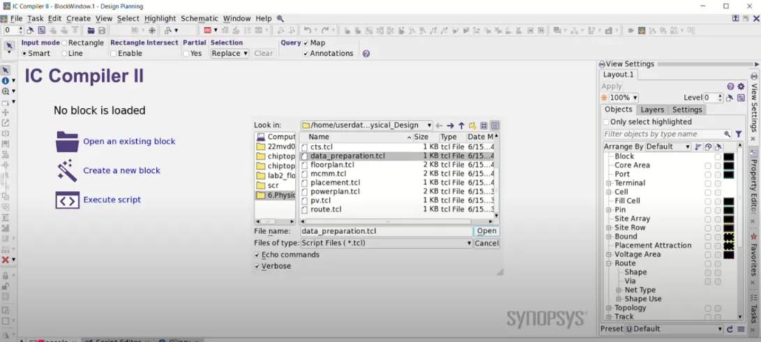
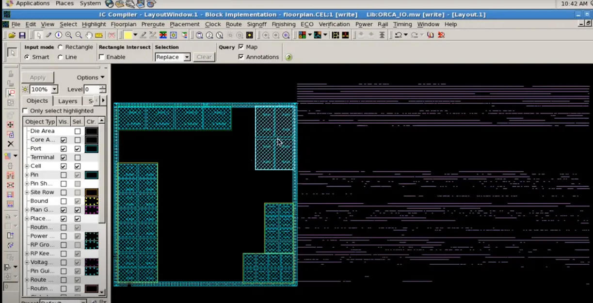
Fig3: shows ICC2 synopsis GUI with design related information loaded and Before placement only macros are placed with respect to reference of data flow
Before placement, macros—large, high-level functional blocks—are strategically positioned in the chip layout, typically with respect to data flow and signal dependencies to optimize performance and reduce interconnection delays. This initial placement considers the logical and physical relationships among macros, ensuring critical data paths are minimized and power distribution is efficient. Module placement without coloring involves positioning functional blocks or modules within the chip layout based solely on their connectivity, size, and design constraints without explicitly assigning different colors or layers to differentiate types of modules or signal types. This approach focuses on achieving an efficient layout by optimizing placement to minimize inter-module interconnect lengths, reduce delays, and improve performance, without the added complexity of layer-specific coloring
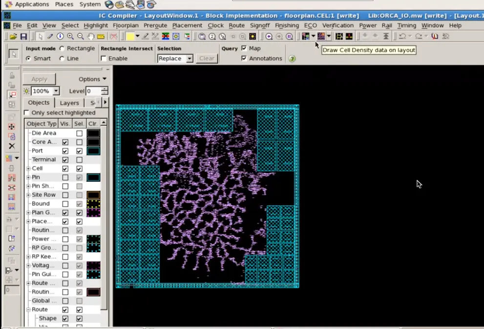
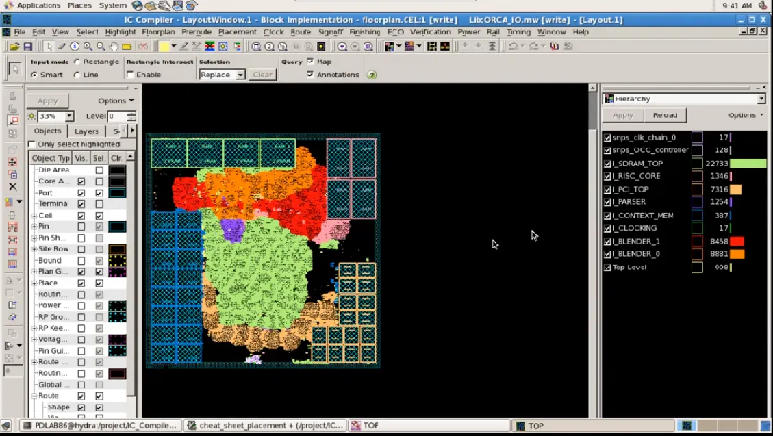
Fig4: Module placement with out colouring and Hierarchical Placement with colouring by each module
Hierarchical placement with coloring by each module involves organizing the placement process into multiple levels, where each module or functional block is assigned a specific color representing its function, type, or hierarchy level. This visual differentiation helps in managing complex designs by clearly identifying different modules and their relationships within the hierarchy.
Placement cell density and pin density congestion maps are tools used in VLSI design to visualize and analyze the distribution of placement cells and pins across the chip area. The placement cell density map shows how densely the placement cells are packed in different regions, helping to identify areas of congestion or underutilization, while the pin density congestion map highlights regions with high concentrations of pins, indicating potential routing challenges and congestion points.
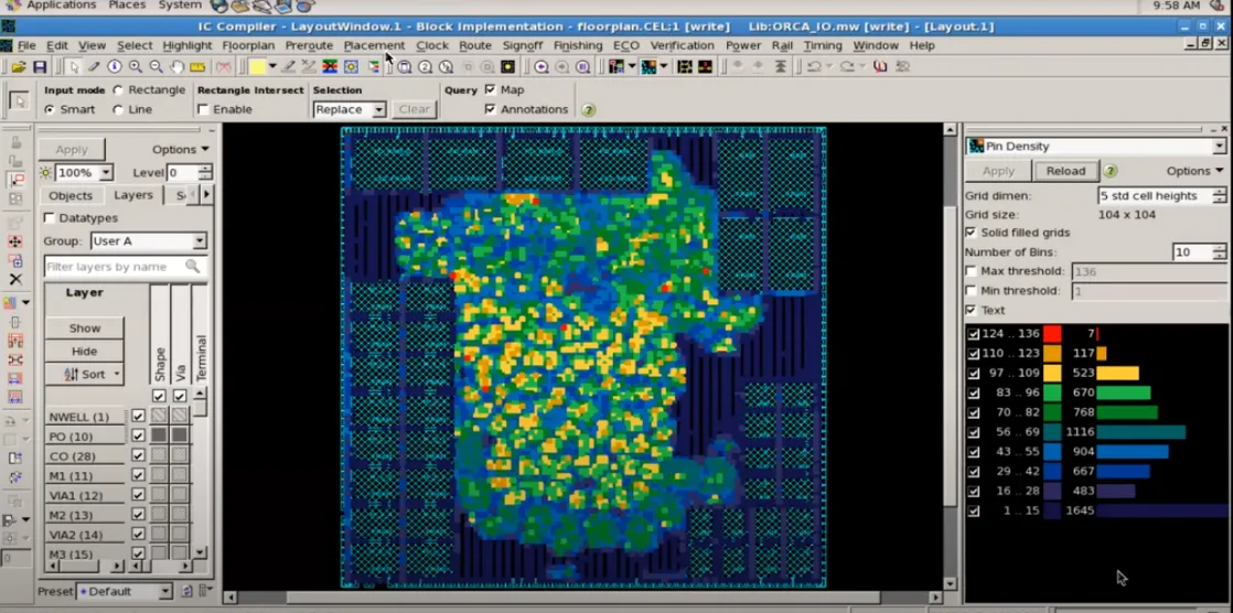
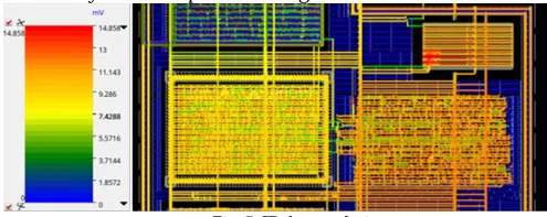
Fig5: placement cell density and Pin density congestion map and IR drop analysis with AI analysis
Strategies for Faster Turnaround Time (TAT)
EDA VENDORS
Major EDA (Electronic Design Automation) vendors in physical design include Synopsys, Cadence Design Systems, Mentor Graphics (now part of Siemens EDA), and ANSYS. These companies provide comprehensive tools and solutions for various stages of physical design, such as placement, routing, parasitic extraction, and sign-off, enabling chip designers to optimize performance, power, and area. Synopsys and Cadence are particularly dominant in the industry, offering widely used platforms like IC Compiler, Innovus, and Allegro, which facilitate efficient physical implementation and verification, thereby playing a crucial role in modern integrated circuit design workflows.
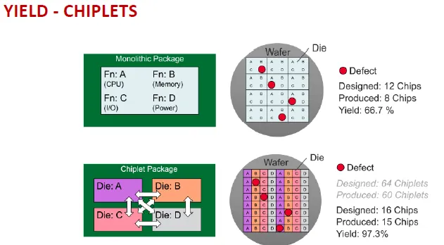
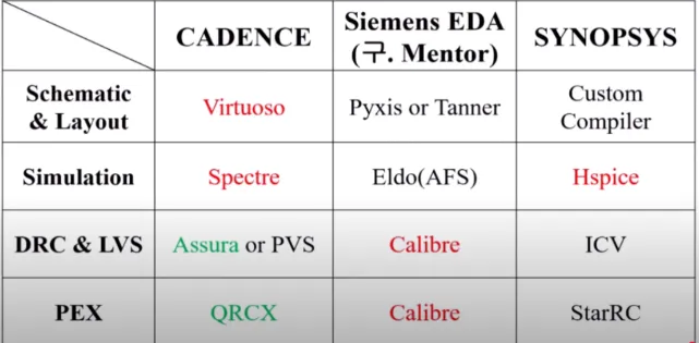
Table 1: Chiplet yield and EDA vendor
Results and Effectiveness
CELL BASED DESIGN
Cell-based design is a methodology in VLSI physical design where complex functional blocks are broken down into pre-designed, reusable standard cells, such as logic gates, flip-flops, and multiplexers, which are then placed and interconnected to create the overall circuit. This approach simplifies the design process, enables automation, and ensures consistency and optimization across different designs. Standard cell libraries provide a set of optimized, pre-characterized cells that can be efficiently used in automated placement and routing tools, making cell-based design the dominant paradigm in modern digital IC design, especially for ASICs and large-scale chips.
ASIC chip fabrication style example
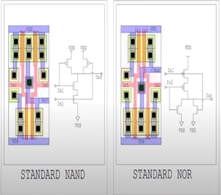
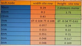
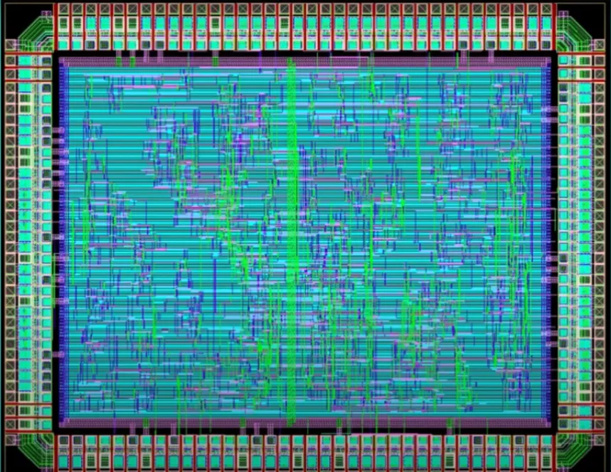
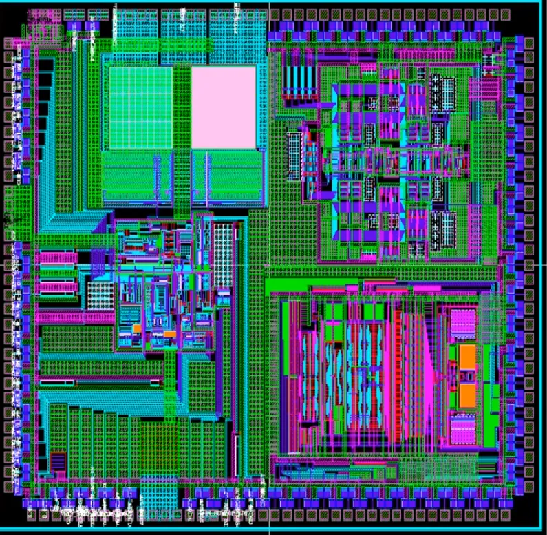
Fig6: Back end physical design soc chip layout
RESULTS AND EFFECTIVENESS
The application of these techniques has shown significant improvements in runtime, memory usage, and PPA metrics in industry designs.AI Initial rail analysis effectively identifies and resolves IR drop issues, enhancing the reliability of the power grid.AI Interleaving placement and optimization has led to reduced CPU time and memory usage compared to traditional methods, demonstrating a more efficient design process.AI Scan-chain reordering has resulted in improved setup and hold slack, indicating enhanced timing performance.
CONCLUSION
The AI Physical design and verification techniques implementation of strategies such as initial power rail analysis, placement optimization interleaving, and scan-chain reordering has significantly reduced design turnaround time in block-level implementations. These methods enhance the quality of runs, allowing for fewer iterations and better performance in lower technology nodes.
This AI research review discusses strategies for optimizing the physical design flow of semiconductor chips, particularly at lower technology nodes, to achieve faster turnaround times (TAT) and improved power, performance, and area (PPA) metrics.
REFERENCES


Venkategowda N.1*, Krishna Koushik2, Ajay Prinstion Pinto3, AI Accelerating The Future ASIC VLSI Chiplet Architecture And Advance EDA, Int. J. Sci. R. Tech., 2026, 3 (8), 431-440. https://doi.org/10.5281/zenodo.21902268
 10.5281/zenodo.21902268