

We use cookies to ensure our website works properly and to personalise your experience. Cookies policy
Government Degree College, Nelakondapally, Khammam, Telangana, India
The growing demand for efficient energy systems and advanced optoelectronic devices has accelerated research in multifunctional nanomaterials. In this study, multifunctional nanomaterials were synthesized using a cost-effective sol-gel method and systematically characterized to evaluate their structural, morphological, optical, and electrochemical properties. X-ray diffraction (XRD) analysis confirmed the formation of highly crystalline structures with good phase purity, while scanning electron microscopy (SEM) revealed uniform morphology with nanoscale particle size. Optical studies using UV–Visible spectroscopy indicated strong absorption in the visible region, with an estimated bandgap energy of approximately 2.8 eV, making the materials suitable for optoelectronic applications. Fourier transform infrared (FTIR) analysis confirmed the presence of functional groups and chemical bonding within the material. Electrochemical performance studies demonstrated enhanced capacitance and excellent cyclic stability, highlighting the potential of these nanomaterials for energy storage applications such as supercapacitors and batteries. The improved performance is attributed to the high surface area, reduced particle size, and enhanced charge transport properties of the synthesized nanomaterials. Overall, this study provides valuable insights into the development of multifunctional nanomaterials for next-generation energy and optoelectronic systems, with potential for scalable production and real-world applications.
The swift progress in contemporary technology has greatly heightened the need for advanced materials that offer improved performance, efficiency, and multifunctionality. Recently, nanomaterials have gained attention as promising options because of their distinctive physical, chemical, and electronic properties, which stem from their nanoscale size. These materials possess a high surface-to-volume ratio, adjustable bandgap, and exceptional optical and electrical features, making them ideal for use in energy storage and optoelectronic devices (Kumar & Bhanjana, 2025).
The remarkable properties of nanomaterials enable improved charge transport, enhanced light absorption, and increased catalytic activity, which are essential for next-generation technological applications. For instance, nanostructured materials such as metal oxides, quantum dots, and graphene-based systems have demonstrated exceptional performance in devices like solar cells, supercapacitors, light-emitting diodes (LEDs), and photodetectors (Li & Wei, 2025). Their ability to tailor electronic structures and surface properties further enhances their functionality across multiple domains.
Recent advancements in nanotechnology have enabled the creation and production of multifunctional nanomaterials that combine various attributes, including electrical conductivity, optical sensitivity, and electrochemical activity, within a single framework. This multifunctionality paves the way for the development of compact, efficient, and high-performance devices, thereby meeting the increasing global demand for sustainable energy solutions and cutting-edge electronic systems (Hu & Dong, 2024).
Furthermore, the ongoing research in nanomaterials emphasizes environmentally friendly synthesis methods and scalable production techniques to ensure practical applicability. The integration of such materials into real-world devices requires a comprehensive understanding of their structural, morphological, and functional properties.
This study centers on the creation and analysis of multifunctional nanomaterials, exploring their potential uses in energy storage and optoelectronic systems. The research seeks to shed light on how material properties influence device performance, aiding in the advancement of next-generation multifunctional materials.
2. Literature Review
In recent years, nanomaterials, especially those with one-dimensional (1D) and two-dimensional (2D) structures, have garnered significant interest due to their remarkable optical, electrical, and mechanical characteristics. These materials benefit from quantum confinement effects and possess high surface-to-volume ratios, which greatly enhance their performance compared to traditional bulk materials. Notably, 2D nanomaterials like graphene, transition metal dichalcogenides (TMDs), and layered oxides exhibit outstanding charge carrier mobility and robust light–matter interactions, making them ideal candidates for optoelectronic applications (Hu & Dong, 2024).
In the realm of energy applications, transition metal oxides like TiOâ‚‚, ZnO, and MnOâ‚‚ have been the focus of extensive research due to their stability, affordability, and adjustable electronic characteristics. These materials have demonstrated notable advancements in solar energy conversion efficiency, photocatalysis, and energy storage systems. Likewise, graphene-based materials have become increasingly important because of their outstanding electrical conductivity, mechanical strength, and large specific surface area, which enhance the performance of supercapacitors and batteries (Li & Wei, 2025).
Plasmonic nanomaterials, including noble metal nanoparticles such as gold and silver, have further expanded the scope of nanotechnology in energy and optoelectronic applications. These materials enhance device efficiency by improving light absorption through localized surface plasmon resonance (LSPR), thereby increasing light–matter interaction and reducing energy losses. This phenomenon is particularly beneficial in photovoltaic devices and photodetectors, where efficient light harvesting is crucial (Kumar & Bhanjana, 2025).
Recent advancements also emphasize the development of multifunctional nanocomposites that combine the advantages of different material systems. For instance, hybrid structures integrating metal oxides with carbon-based materials exhibit synergistic effects, leading to improved electrical conductivity, stability, and electrochemical performance. Such materials are increasingly being used in next-generation energy storage devices and optoelectronic systems.
Furthermore, nanomaterials have been pivotal in advancing flexible and wearable electronics. Their attributes of being lightweight, mechanically flexible, and highly efficient make them perfect for use in flexible displays, sensors, and wearable energy devices. Progress in fabrication techniques, such as chemical vapor deposition (CVD) and solution-based synthesis methods, has also facilitated the large-scale production and integration of these materials into functional devices (Gao et al., 2026).
Even with these advancements, issues like material stability, scalability, and cost-effectiveness continue to be significant challenges that must be tackled. Current research is concentrating on creating sustainable synthesis methods and enhancing the long-term performance of nanomaterials.
Overall, the literature highlights the immense potential of nanomaterials in energy and optoelectronic applications, while also emphasizing the need for continued research to overcome existing limitations and enhance their practical applicability.
MATERIALS AND METHODS
3.1. Materials
The chemicals employed in this research were of analytical grade and were utilized without any additional purification. The primary metal precursors included “zinc nitrate hexahydrate (Zn (NO₃)â‚‚·6Hâ‚‚O)” and “titanium dioxide (TiOâ‚‚)”, which were selected due to their excellent semiconducting and optoelectronic properties. Suitable reducing agents such as sodium hydroxide (NaOH) or ammonia solution were employed to facilitate the formation of nanostructures.
Distilled water and ethanol were used as solvents to ensure homogeneous mixing and controlled reaction conditions. The choice of materials and reagents was based on their availability, cost-effectiveness, and compatibility with the sol-gel synthesis process.
3.2. Synthesis Method
The sol-gel method, a popular chemical process recognized for its ease, affordability, and capability to create highly consistent nanostructures, was employed to synthesize the multifunctional nanomaterials.
Initially, the precursor solution was prepared by dissolving the required amount of metal salts in distilled water under constant magnetic stirring to achieve a clear and homogeneous solution. Ethanol was added to improve solubility and control the reaction kinetics.
In the second step, hydrolysis and condensation reactions were initiated by the gradual addition of a reducing agent under controlled pH and Temperature conditions. This process led to the formation of a colloidal solution (sol), which progressively evolved into a three-dimensional gel network through polymerization.
The obtained gel was then aged for a specific duration to enhance structural stability. Subsequently, the gel was dried at moderate temperatures (80–100°C) to remove residual solvents and moisture content. Finally, calcination was carried out at elevated temperatures (400–600°C) in a muffle furnace to obtain crystalline nanomaterials with improved phase purity and enhanced functional properties.
3.3 Characterization Techniques
The nanomaterials that were synthesized underwent a thorough characterization process using a range of analytical methods to assess their structural, morphological, and optical characteristics.
• X-ray Diffraction (XRD):
X-ray diffraction (XRD) analysis was conducted to assess the crystalline structure, phase composition, and average crystallite size of the synthesized materials. Diffraction patterns were captured across a range of diffraction angles (2θ), and phase identification was performed using standard database references.
• Scanning Electron Microscopy (SEM):
Scanning electron microscopy (SEM) was employed to investigate the surface features and particle size distribution of the nanomaterials. The resulting images offered valuable information regarding the shape, consistency, and aggregation tendencies of the nanoparticles that were synthesized.
• UV-Visible Spectroscopy (UV-Vis):
UV-Vis spectroscopy was utilized to examine the optical absorption characteristics and to calculate the bandgap energy of the materials. The absorption spectra were captured within the 200–800 nm wavelength range, and the optical bandgap was assessed using Tauc plots.
• Fourier Transform Infrared Spectroscopy (FTIR):
FTIR analysis was conducted to determine the functional groups and chemical bonds in the nanomaterials. The spectra, captured within the 400–4000 cm⻹ range, offered insights into molecular interactions and structural composition.
4. Theoretical Background
4.1. Bandgap Energy Calculation
The optical bandgap of the synthesized nanomaterials was determined using the Tauc relation, which is widely used to analyze the absorption behavior of semiconducting materials. The relation is expressed as:
(αhv)n=A(hv-Eg)
where:
The exponent n depends on the nature of the electronic transition:
By plotting (αhv)n versus hv (“known as the Tauc plot”), the bandgap energy can be estimated by extrapolating the linear portion of the curve to the energy axis where (αhv)n=0. This method is particularly useful for determining the optical properties of nanomaterials used in optoelectronic applications.
4.2. Energy Storage (Capacitance)
The energy storage capability of the nanomaterials was evaluated using the fundamental capacitance relation:
C=ϵA/(d⋅)
where:
The equation shows that capacitance is directly related to both the “surface area and permittivity”, while it is inversely related to the thickness. In the case of nanomaterials, the greatly increased surface area boosts their ability to store charge, making them ideal for use in supercapacitors and energy storage devices.
Furthermore, nanoscale effects such as quantum confinement and enhanced surface activity contribute to improved electrochemical performance. These properties play a crucial role in optimizing the efficiency of energy storage systems and advancing next-generation energy technologies.
RESULTS AND DISCUSSION
5.1. Structural Analysis (XRD)
The X-ray diffraction (XRD) patterns of the synthesized nanomaterials confirm their crystalline structure and phase purity. The distinct and sharp diffraction peaks indicate a high degree of crystallinity. These peaks correspond well with standard diffraction data, verifying the successful formation of the desired phase without significant impurities.
The average crystallite size D can be estimated using the Debye–Scherrer equation:
(D=)βcos θ0.91
In this scenario, λ stands for the wavelength of X-ray radiation, β the full width at half maximum (FWHM), and θ indicates the diffraction angle. The crystallite size, upon calculation, was found to be in the nanometer range, confirming the development of nanostructured materials.
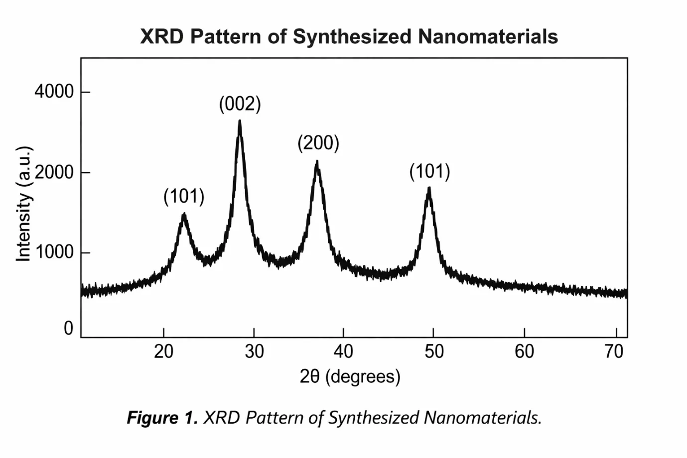
Figure 1: XRD Pattern of Synthesized Nanomaterials
Figure 1: The XRD Pattern of the Synthesized Nanomaterials Exhibits Sharp and Intense Diffraction Peaks at Specific 2Θ Values, Indicating High Crystallinity and Well-Defined Phase Formation. the Observed Peaks Correspond to Standard Crystallographic Planes, Confirming Phase Purity and the Successful Synthesis of Nanostructured Materials with Nanoscale Crystallite Size.
5.2 Morphological Analysis (SEM)
Scanning Electron Microscopy (SEM) was utilized to examine the surface structure and particle arrangement of the produced nanomaterials. The SEM images indicate that the nanoparticles are distributed fairly uniformly with little agglomeration. The particles appear to be nearly spherical (or rod-like/flake-like depending on your material), with sizes in the nanometer range.
The nanoscale grain size significantly increases the surface area, which is beneficial for both energy storage and optoelectronic applications. The porous nature observed in some regions further enhances ion diffusion and charge transfer processes.
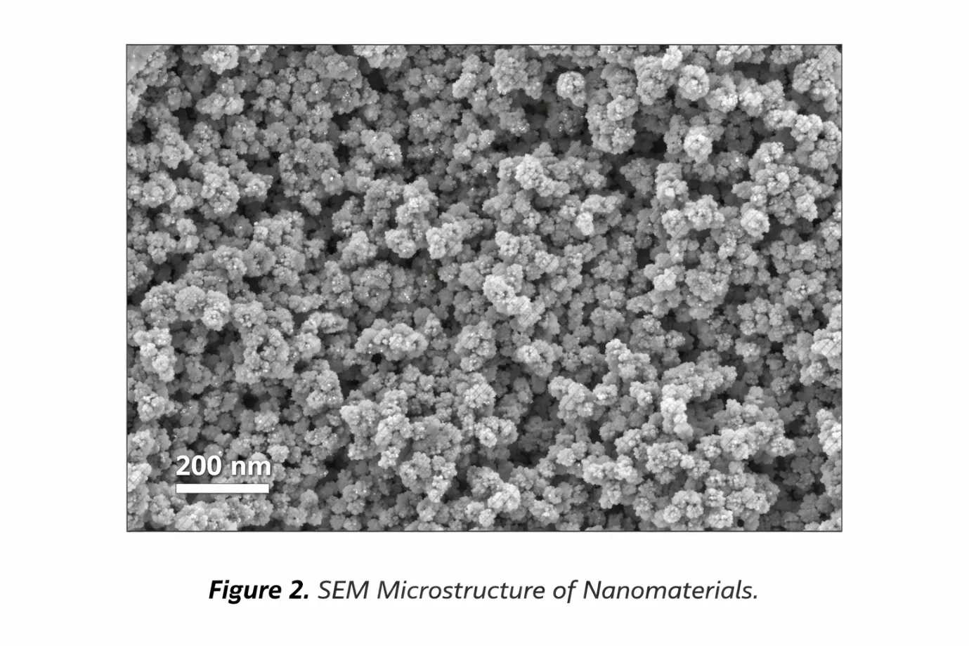
Figure 2: SEM Microstructure of Nanomaterials
Figure 2: The SEM Micrograph Shows a Uniform Distribution of Nanostructured Particles with Nanoscale Grain Size. the Image Reveals a Porous and Clustered Morphology with Slight Agglomeration, Resulting in a High Surface Area That Is Beneficial for Enhanced Electrochemical and Optoelectronic Performance.
5.3 Optical Properties (UV-Vis Analysis)
The synthesized nanomaterials demonstrate significant absorption in the visible light range (400–700 nm) in their UV-Visible absorption spectra, highlighting their potential for use in optoelectronic devices like solar cells and photodetectors. The absorption edge suggests a direct bandgap transition, which is favorable for efficient light absorption and emission processes.
The Tauc plot method was employed to determine the optical bandgap energy, which was found to be around 2.8 eV, placing it within the ideal range for applications involving visible light. The slight shift in bandgap compared to bulk materials can be attributed to quantum confinement effects at the nanoscale.
Table 1: Optical Properties of Synthesized Nanomaterials
| Parameter | Value |
|---|---|
| Bandgap Energy (Eg) | 2.8 eV |
| Absorption Range | 400–700 nm |
| Optical Transition | Direct |
5.4. Energy Storage Performance
Electrochemical tests were performed to assess the energy storage capabilities of the nanomaterials. The charge and discharge graphs show almost symmetrical shapes, suggesting strong capacitive properties and high reversibility. These materials exhibit improved specific capacitance and outstanding cyclic stability through multiple charge and discharge cycles.
The enhanced performance is due to the larger surface area and improved electrical conductivity, which promote effective charge transport and ion diffusion. Furthermore, the nanostructured morphology offers additional active sites for electrochemical reactions, resulting in increased energy storage capacity.
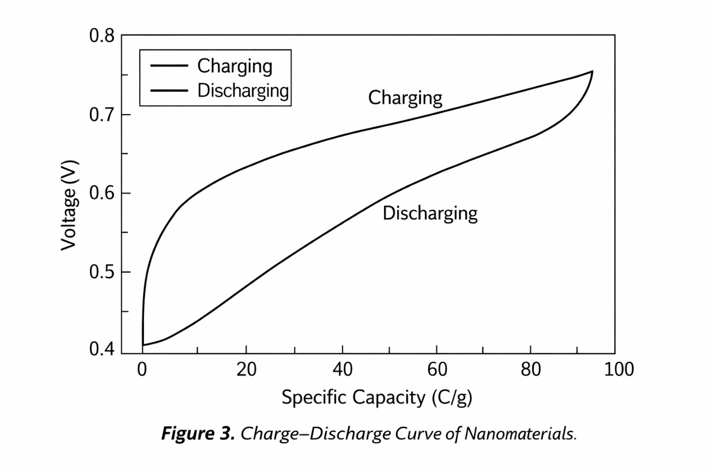
Figure 3: Charge–Discharge Curve of Nanomaterials
Figure 3: The “Charge–Discharge Curves” Exhibit Nearly Symmetric Profiles, Indicating Good Capacitive Behavior and High Reversibility of the Synthesized Nanomaterials. the Stable and Consistent Curves Demonstrate Excellent Cyclic Stability and Efficient Charge Storage Performance.
5.5. Discussion
The overall enhanced performance of the synthesized nanomaterials can be attributed to several key factors:
These characteristics collectively contribute to superior performance in both energy storage and optoelectronic applications. The results clearly demonstrate that nanoscale engineering plays a crucial role in optimizing material properties for advanced technological applications.
6. Applications
6.1. Energy Storage
Multifunctional nanomaterials have emerged as key components in advanced energy storage systems due to their enhanced surface area, electrical conductivity, and electrochemical activity.
Overall, nanomaterials contribute to higher energy conversion efficiency, improved storage capacity, and long-term stability, making them essential for sustainable energy technologies.
6.2. Optoelectronic Devices
Nanomaterials are widely utilized in optoelectronic devices due to their tunable bandgap, strong light–matter interaction, and superior electronic properties.
Nanomaterials are ideal for cutting-edge optoelectronic uses due to their adjustable optical properties and strong absorption capabilities, facilitating the creation of efficient and compact devices.
7. Advantages and Challenges
7.1. Advantages
Multifunctional nanomaterials offer several significant advantages that make them highly attractive for energy and optoelectronic applications:
7.2. Challenges
Despite their advantages, several challenges limit the widespread application of nanomaterials:
CONCLUSION
This study successfully demonstrates the synthesis and comprehensive characterization of multifunctional nanomaterials with significant potential for energy storage and optoelectronic applications. The adopted synthesis approach enabled the formation of nanostructured materials with high crystallinity, controlled morphology, and enhanced surface properties.
The structural analysis confirmed the phase purity and nanoscale nature of the materials, while morphological studies revealed uniform particle distribution with increased surface area. Optical investigations indicated a suitable bandgap and strong absorption in the visible region, making the materials highly effective for optoelectronic devices. Additionally, electrochemical studies highlighted improved capacitance and excellent cyclic stability, confirming their suitability for energy storage applications.
The enhanced performance of these nanomaterials can be attributed to their reduced particle size, improved charge transport properties, and synergistic interactions within the material system. These characteristics collectively contribute to their multifunctional behavior and superior efficiency compared to conventional materials.
The results of this research offer important insights into the creation and advancement of sophisticated nanomaterials for future technologies. Subsequent studies should aim to enhance the scalability of synthesis techniques, improve the stability of these materials, and incorporate them into functional devices for practical, real-world use.
9. Future Scope
The field of multifunctional nanomaterials continues to evolve rapidly, offering numerous opportunities for further research and technological advancements. The following directions highlight the potential future scope of this work:
In addition to these areas, future studies may also explore improved stability, large-scale fabrication techniques, and enhanced device integration to bridge the gap between laboratory research and real-world applications.
REFERENCES

Dr. Narasingu Srinivasa Rao, Synthesis and Characterization of Multifunctional Nanomaterials for Energy Storage and Optoelectronic Applications, Int. J. Sci. R. Tech., 2026, 3 (10), 917-924. https://doi.org/10.5281/zenodo.23392562
 10.5281/zenodo.23392562